The Self-Driving Lab: How AI is Revolutionizing Chip Design from Floorplan to Route
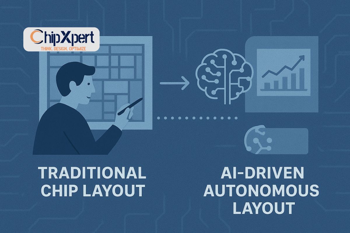
physical chip design has been a monumental task of human ingenuity. Engineers, armed with powerful EDA tools, would spend weeks or months painstakingly crafting a chip’s floorplan, placing millions of cells, and routing a maze of interconnections—all while battling the relentless constraints of Power, Performance, and Area (PPA).
It was a craft. But now, it’s becoming a science—powered by artificial intelligence.
The EDA industry is undergoing a seismic shift. Machine Learning (ML) is no longer a buzzword; it’s actively embedded in the tools that design the world’s most advanced chips. At ChipXpert, we’re preparing the next generation of VLSI engineers for this new reality. Let’s explore how AI is revolutionizing the core stages of physical design.
From Heuristics to Learning: The Old Way vs. The New Way
Traditionally, EDA tools relied on complex heuristic algorithms and cost functions. Engineers would run a tool, analyze the result, tweak hundreds of knobs and constraints, and run it again—an iterative, time-consuming process heavily dependent on expert intuition.
AI/ML changes the game. Instead of just following pre-defined rules, these tools can now:
- Learn from vast datasets of previous successful chip designs.
- Predict outcomes (like timing or congestion) before committing to a long, compute-intensive process.
- Autonomously explore the design space to find solutions humans might never consider.
This isn’t about replacing the engineer; it’s about augmenting them with a powerful, data-driven co-pilot.
1. AI-Driven Floorplanning: The Strategic Blueprint
The floorplan is the most critical strategic decision in physical design. A poor floorplan can doom a project. AI is transforming this in two key ways:
- Predictive Modeling: ML models can analyze a netlist and predict optimal macro placement, power network architecture, and overall chip shape to avoid congestion and timing issues later. They can answer “what-if” scenarios in minutes instead of days.
- Generative Design: Instead of a single floorplan, AI can generate thousands of potential floorplan alternatives, each optimized for a different PPA goal (e.g., maximize performance vs. minimize area). The designer can then choose the best strategic option. Tools like Synopsys DSO.ai™ are pioneers in this space, acting as an autonomous design assistant for global exploration.
2. Intelligent Placement: Where to Put Every Gate
Placement decides the exact location of every standard cell. The goal is to minimize total wirelength and avoid congestion while meeting timing constraints. It’s a problem with astronomically large possible permutations.
- Reinforcement Learning (RL) in Action: AI placement engines use RL to learn the optimal placement of cells. They treat placement as a game: the “action” is placing a cell, the “reward” is improved wirelength, reduced congestion, and better timing. By playing this game millions of times, the AI learns a winning strategy. This leads to more optimal, human-like placements without human-level runtime.
- Congestion Prediction: ML models can accurately routing congestion hotspots based on early placement data. This allows the tool to proactively spread cells and avoid problems before the slow and complex routing stage even begins.
3. Smarter Routing: Connecting the Billions of Dots
Routing is the final, intricate step of connecting all the placed cells according to design rules. It’s perhaps the stage seeing the most dramatic AI infusion.
- Predicting and Fixing Timing Violations: ML models can predict post-route timing (setup/hold) and signal integrity issues (like crosstalk) from pre-route data. This allows the tool to fix potential problems during placement and early routing stages, preventing a costly iterative loop at the end.
- Optimizing for Multiple Objectives: Traditional routers focus on connecting wires without violating rules. AI-driven routers can simultaneously optimize for timing, power, signal integrity, and manufacturability (DFM), finding a superior global optimum across all these competing constraints.
The Tangible Benefits: Why It Matters
This AI revolution isn’t academic; it delivers real, measurable results:
- Superior PPA: AI can find solutions that improve performance by 10-20% or reduce power consumption by a similar margin compared to traditional flows.
- Dramatically Reduced Turnaround Time (TAT): What took weeks of iterative tweaking can now be achieved in days. This acceleration is crucial for meeting tight market windows.
- Democratizing Expertise: AI tools encapsulate the knowledge of expert designers, helping less experienced engineers achieve expert-level results. This helps address the global talent gap in chip design.
The Future is Autonomous
The trajectory is clear. We are moving from assisted design to autonomous design. The future VLSI engineer will be a conductor of an AI orchestra, setting high-level goals and constraints (“optimize for low power”), and letting the AI tools determine the best way to achieve them.
Learn to Partner with AI at ChipXpert
The role of the VLSI engineer is evolving. The most sought-after professionals will be those who understand both the foundational principles of physical design and how to effectively leverage AI-driven tools.
At ChipXpert, our advanced VLSI curriculum is designed to bridge this gap. We provide the deep foundational knowledge of timing, power, and layout that is essential to understand what the AI is doing and why, empowering you to guide it effectively.
Ready to master the tools that are defining the future of chip design? Explore our Physical Design training program and learn how to harness the power of AI to build better chips, faster.


