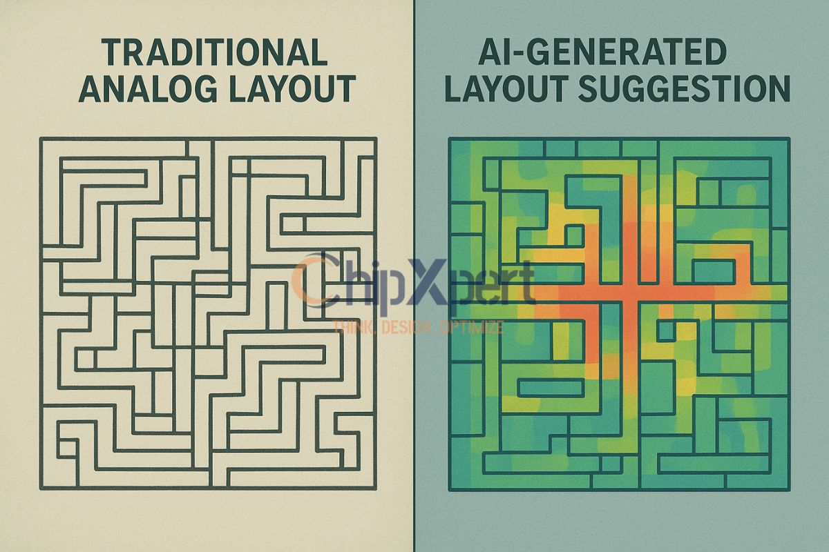
The Analog Artisan’s New Apprentice: Can AI Finally Automate Analog Layout?
Analog Layout has been a craft. It’s a discipline of intuition, where engineers meticulously hand-place transistors, weave routing to minimize parasitic coupling, and arrange components like a master watchmaker assembling a delicate movement. It’s slow, painstaking, and deeply human. But whispers of change are echoing through the EDA industry: AI-driven automation is coming for analog layout.
The promise is seductive: push a button and an AI generates a perfectly optimized, DRC-clean analog block in hours, not weeks. But is this the reality? At ChipXpert, we’re dissecting the hype to understand the true impact of automation on the analog artisan’s craft. Let’s explore the promise, the reality, and the future of AI in analog place and route.
The Grand Promise: Why Automate Analog Layout?
The drivers for automation are powerful:
- The Productivity Paradox: While digital design has been fully automated for years, analog layout remains stubbornly manual. This creates a massive bottleneck in mixed-signal SoC design, slowing time-to-market for everything from smartphones to electric cars.
- The Complexity Cliff: Advanced nodes (FinFET, GAA) have made analog layout infinitely more complex. Managing matching, parasitics, and DFM rules in a 3D environment is pushing human capabilities to the limit.
- The Optimization Ceiling: A human designer can create a good, working layout. But can they find the optimal one? AI promises to explore the design space more exhaustively, finding layouts that are not just correct, but are superior in performance, power, and area (PPA).
The Sobering Reality: Why Analog is the “Final Frontier” of Automation
Despite the hype, full automation remains a distant goal. The challenges are profound:
- The “Fuzzy” Rules of Analog: Digital P&R follows clear, binary rules: timing closure and DRC-clean. Analog success is measured in gradients and trade-offs: “good enough” matching, “acceptable” noise, “sufficient” bandwidth. Translating these nuanced, often conflicting, goals into a cost function for an AI is incredibly difficult.
- The Know-How Problem: An expert layout engineer’s decisions are based on decades of accumulated tacit knowledge—lessons from past failures and an intuitive feel for the silicon. Capturing this “black art” into an algorithm is the core challenge.
- The Setup Overhead: Configuring an AI-driven tool is often a complex project in itself. You must define constraints, weighting priorities, and cost functions with extreme precision. A poorly defined problem will lead to a poorly generated layout. It often requires as much expertise as doing the layout manually.
How AI is Actually Helping Today: The “Co-Pilot” Model
While full automation isn’t here, AI is delivering real value as a powerful design assistant or co-pilot. The current reality is about augmentation, not replacement.
- Topology Planning and Prototyping: AI can rapidly generate multiple floorplanning options for an analog block. A designer can then review these suggestions, select the most promising candidate, and then refine it manually. This solves the “blank canvas” problem and sparks new ideas.
- Intelligent Placement Assistance: AI tools can now handle the tedious, rule-heavy aspects of placement:
- Matching Engine: Automatically arranging devices in common-centroid or interdigitated patterns while adhering to complex FinFET rules (dummy fins, stress effects).
- Constraint Generation: Automatically detecting differential pairs and current mirrors in the schematic and generating matching and symmetry constraints for the layout tool.
- Parasitic-Aware Optimization: This is a killer app in the making. AI can predict parasitic capacitance and resistance during placement and routing, not after. It can then iteratively adjust the layout to minimize these parasitics, something a human can only do through slow, iterative guesswork.
- Routing Guidance: Instead of full auto-routing, AI can highlight optimal routing paths to avoid noise-sensitive nodes, suggest shielding strategies, and ensure symmetric routing for critical signals—dramatically reducing the time spent on this error-prone task.
The EDA Landscape: Tools to Watch
The market is evolving rapidly. Tools from established players like Cadence (with its Cerebrus AI technology) and startups are offering varying levels of automation, from assisted placement to full-flow solutions that take a netlist and generate a layout. The key is to understand their limitations and that they require significant expert oversight.
What This Means for the Analog Layout Engineer
The rise of AI doesn’t spell the end of the analog layout engineer; it signals an evolution of the role.
- From Artisan to Conductor: The engineer will spend less time on manual polygon pushing and more time on high-level strategy: defining constraints, guiding the AI, verifying results, and making complex trade-off decisions.
- Increased Value of Fundamentals: Understanding device physics, parasitic effects, and noise mechanisms becomes more important, not less. You need this knowledge to properly guide the AI and judge its output.
- The Need for New Skills: Proficiency with these new AI-driven EDA tools will become a highly valuable skill in the job market.
Future-Proof Your Skills at ChipXpert
The future belongs to engineers who can blend classic analog design intuition with the power of modern AI-driven tools.
At ChipXpert, our Analog Layout training program is designed for this future. We provide the unshakable foundation in device physics and layout techniques that you will always need, while also introducing the concepts and tools that are defining the next era of design.
Ready to become the conductor of your own AI-powered design flow? Explore our Analog Layout training program and learn the skills that will keep you at the forefront of the industry.


