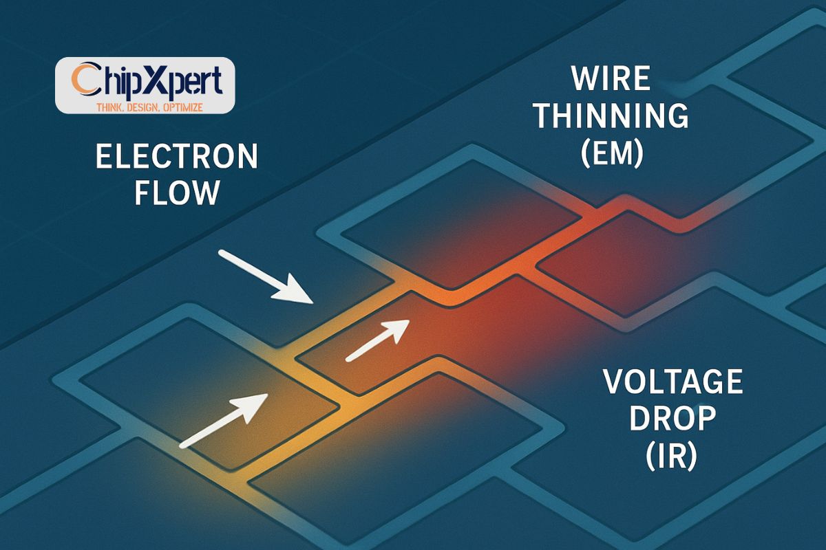
The Silent Killers: Why Electromigration and IR Drop Analysis is Non-Negotiable for Chip Sign-Off
In the high-stakes world of chip design, some failures are dramatic and immediate. Others are silent, slow, and insidious. A chip can pass every functional test in the lab, ship to a customer, and then fail years later for no apparent reason. The culprits? Often, it’s the silent killers of power integrity: Electromigration (EM) and IR Drop.
For designs at advanced nodes—especially high-performance processors and ultra-low-power IoT devices—ignoring these phenomena is not an option. They are absolutely critical sign-off considerations, as important as timing closure. At ChipXpert, we ensure our students understand that robust physical design isn’t just about timing; it’s about ensuring the chip lives a long and healthy life. Let’s demystify these two critical challenges.
1. Electromigration (EM): The Slow Erosion
Imagine a crowded highway during rush hour. Over time, the constant flow of cars causes wear and tear on the road. Electromigration is similar, but for the microscopic wires (interconnects) in your chip.
- What it is: Electromigration is the gradual displacement of metal atoms due to the momentum transfer from high-density electron flow. Over time, this can cause:
- Voids: Thinning of wires, leading to increased resistance and eventual open circuits.
- Hillocks: Accumulation of atoms, leading to bulges that can cause short circuits to adjacent wires.
- Why it’s a bigger problem now: At advanced nodes, wires are narrower, and current densities are higher. This dramatically accelerates the EM process. A wire that would have lasted decades at 90nm might fail in mere months at 7nm.
- The Analogy: It’s like the “metal fatigue” of your chip’s wiring. You won’t see it on day one, but it will cause a catastrophic failure down the line.
2. IR Drop: The Brownout Effect
Now, imagine that same crowded highway, but now it’s built with tiny, resistive roads. The further you travel, the more energy is lost. This is IR Drop.
- What it is: IR Drop is the voltage loss that occurs as current flows through the resistance (R) of the power delivery network (PDN). This means the voltage that arrives at a transistor is less than the voltage supplied at the chip’s pad.
- Why it’s critical: Transistors are designed to operate within a specific voltage range. Excessive IR drop can cause:
- Performance Loss (Slowdown): Lower voltage leads to longer transistor switching delays, causing timing violations and reducing the chip’s maximum operating frequency.
- Functional Failure: In severe cases, the voltage can drop so low that logic gates stop switching correctly, leading to silent data corruption—the worst kind of bug.
- The Analogy: It’s like a “brownout” in a city. The lights might still be on, but they’re dim, and appliances don’t work properly.
The Vicious Cycle: How EM and IR Drop Feed Each Other
These two phenomena are not independent; they create a dangerous feedback loop:
- EM causes voids in wires.
- These voids increase the resistance (R) of the wire.
- According to Ohm’s Law (V = I * R), this increased resistance leads to a larger IR Drop for the same amount of current (I).
- To compensate for the performance loss from IR drop, a system might try to increase the voltage, which in turn increases the current (I).
- This higher current accelerates the Electromigration process, creating more voids.
This cycle can lead to a rapid and catastrophic failure.
Taming the Beasts: Sign-Off Strategies
Passing EM and IR sign-off requires a proactive, multi-faceted approach throughout the physical design flow:
For Electromigration (EM):
- Wider Wires: Use wider power straps for global routes where current density is highest.
- Abundant Vias: A single via can be an EM hotspot. Using double-cut vias or multiple vias at connections significantly reduces current density per via.
- Advanced Metallurgy: Foundries provide specific design rules for different metal layers and offer EM-aware wire libraries.
- Dynamic Analysis: Beyond standard DC analysis, average current and transient EM analysis are needed to account for real switching activity.
For IR Drop Analysis:
- A Robust Power Delivery Network (PDN): This is the first line of defense. Design a dense, mesh-like grid of power and ground lines to provide low-resistance paths.
- Strategic Decap Placement: Decoupling capacitors act as tiny local charge reservoirs. They supply instantaneous current to nearby logic, suppressing local IR drop during switching events. Placing them close to high-switching logic blocks is crucial.
- Power-Aware Placement: Avoid placing all high-power cells in one area. Spread them out to prevent localized IR drop hotspots.
- Static vs. Dynamic Analysis:
- Static IR Drop: A conservative, vector-less analysis that assumes all gates can switch simultaneously. It’s a good first check.
- Dynamic IR Drop: The gold standard. It uses the actual switching activity from VCD files to simulate the voltage drop over time. This is essential for accurate sign-off, as it identifies issues missed by static analysis.
What This Means for the VLSI Engineer
Gone are the days when power integrity was an afterthought. Today’s physical design and sign-off engineer must:
- Think like a power network architect from the floorplanning stage.
- Master EM/IR analysis tools and know how to interpret their results.
- Understand the physics of failure to make intelligent design trade-offs.
Build Sign-Off Expertise at ChipXpert
Mastering EM and IR drop is not just about running a tool; it’s about understanding the underlying principles to make smart design decisions that ensure reliability.
At ChipXpert, our advanced Physical Design training curriculum places a heavy emphasis on power integrity and sign-off checks. We provide the foundational knowledge and practical skills needed to design robust, reliable chips that won’t fall victim to these silent killers.
Ready to master the critical checks that separate a working chip from a reliable one? Explore our Physical Design training program and learn the art and science of sign-off from industry experts.


