From RTL to Tapeout : A Complete VLSI Flow Explained
The journey from an idea to a working silicon chip is a fascinating and complex process. For those aspiring to build a career in VLSI (Very-Large-Scale Integration) design, understanding the end-to-end flow from RTL to Tapeout is not just essential—it’s foundational. This blog aims to demystify this process and explain each stage in a simple, humanized manner for students and young engineers who are starting their journey into the world of semiconductors.
At ChipXpert Technologies Pvt. Ltd. (www.chipxpert.in), a leading VLSI training institute in India, we offer detailed, hands-on training programs designed to help students understand and implement these concepts in real-world scenarios.
What is RTL to Tapeout Flow in VLSI?
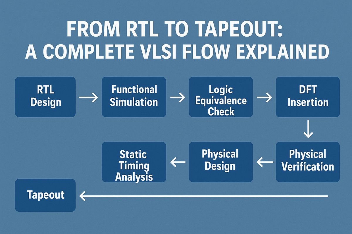
In VLSI, the term “RTL to Tapeout” refers to the complete process of taking a hardware design from its Register Transfer Level (RTL) description, typically written in Verilog or VHDL, all the way to GDSII (tapeout)—the final data sent for fabrication. This flow involves multiple stages, each requiring its own specialized tools, methodologies, and expertise.
Why Understanding This Flow is Important
For VLSI aspirants, understanding the flow helps in choosing the right career path—whether it’s Design Verification, Physical Design, DFT, or Analog Layout. Knowing how each block fits together gives clarity on how the semiconductor industry functions as a whole.
At ChipXpert, we integrate this holistic knowledge into our Physical Design, Design Verification, Analog Layout, and DFT training programs. Explore Courses
Step-by-Step Explanation of RTL to Tapeout Flow
1️⃣ Specification and Architecture
The process begins with defining the specifications—what the chip is supposed to do, power targets, performance goals, area constraints (PPA), and so on. Based on this, architects outline the block diagrams and high-level structure.
2️⃣ RTL Design (Register Transfer Level)
RTL design involves coding the intended functionality in HDLs (Hardware Description Languages) like Verilog or VHDL. This stage focuses on creating the logic that defines how data moves through the design based on clock cycles.
Outcome: A synthesizable RTL code.
Tools: Synopsys Design Compiler, Cadence Genus.
3️⃣ Functional Verification
Before moving ahead, it’s crucial to verify that the RTL design functions correctly. This is where Design Verification (DV) comes in. Engineers write testbenches and run simulations to catch functional bugs.
Popular Verification Techniques:
- Simulation (using tools like Cadence Xcelium, Synopsys VCS)
- Formal Verification
- UVM (Universal Verification Methodology)
Outcome: Functionally verified RTL.
Read More: Design Verification Course at ChipXpert
4️⃣ Synthesis
Synthesis transforms the RTL into a gate-level netlist using standard cells from a technology library. This step ensures the logic is mapped to physical components.
Key Considerations:
- Timing constraints (SDC)
- Area and power optimizations
- DFT structures (Scan Chains, MBIST insertion)
Outcome: Gate-level netlist.
Tools: Synopsys Design Compiler, Cadence Genus.
5️⃣ Static Timing Analysis (Pre-Layout)
Before physical implementation, perform an initial Static Timing Analysis (STA) on the synthesized netlist to ensure it meets timing constraints.
Tools: Synopsys PrimeTime.
6️⃣ Design for Testability (DFT) Insertion
At this stage, additional logic is added to make the chip testable after fabrication. This includes scan chains, MBIST (Memory Built-in Self-Test), and BIST (Built-in Self-Test).
Outcome: Testable gate-level netlist.
Explore: DFT Course at ChipXpert
7️⃣ Physical Design (PD)
This is where the magic of translating a logical design into a physical chip layout happens.
Key Stages:
- Floorplanning: Plan the die size, place macros, define power grids.
- Placement: Position standard cells optimally.
- Clock Tree Synthesis (CTS): Build clock distribution networks for minimal skew.
- Routing: Connect cells using metal layers while optimizing for congestion and timing.
Tools: Cadence Innovus, Synopsys ICC2.
8️⃣ Physical Verification (PV)
After placement and routing, the design undergoes multiple verification steps:
- DRC (Design Rule Check): Ensures the design follows foundry rules.
- LVS (Layout vs Schematic): Confirms that the physical layout matches the logical netlist.
- ERC (Electrical Rule Check): Verifies electrical integrity.
Tools: Mentor Graphics Calibre.
Read: Physical Design Course at ChipXpert
9️⃣ Signoff
Before tapeout, the design undergoes signoff analysis:
- STA (Post-layout)
- IR Drop and EM Analysis
- Noise Analysis
- Parasitic Extraction
- Power Analysis
Signoff ensures that the design is fabrication-ready and free from critical issues.
1 Tapeout (GDSII Generation)
Finally, the verified and signed-off design is converted into GDSII format. This data is sent to the foundry for manufacturing. This stage is called tapeout—the final checkpoint in the VLSI design flow.
How This Flow Fits into Industry Roles
Understanding this flow helps students map industry job roles more clearly:
- RTL Design Engineer: Focuses on RTL coding and synthesis.
- Verification Engineer: Ensures functional correctness through simulations.
- DFT Engineer: Adds and verifies test structures.
- Physical Design Engineer: Handles floorplanning to routing and signoff.
- Analog Layout Engineer: Works on the custom layout blocks integrated with digital.
Why Choose ChipXpert for VLSI Training?
At ChipXpert Technologies Pvt. Ltd., we don’t just teach theory—we bridge the gap between academics and industry through hands-on, tool-based, and project-driven learning. Our students graduate with skills directly applicable to industry-standard VLSI workflows.
🔗 Explore Our Popular Training Programs:
- VLSI Physical Design Course
- VLSI Design Verification Course
- Advanced Analog Layout Course
- Design for Testability (DFT) Course
Final Thoughts
The RTL to Tapeout flow is at the heart of semiconductor innovation, powering everything from smartphones to AI accelerators. Mastering this flow is essential for anyone serious about a career in VLSI design.
At ChipXpert, we ensure you don’t just learn it—you live it through real projects, practical tools, and mentorship from industry veterans.
Your VLSI career starts here: www.chipxpert.in
