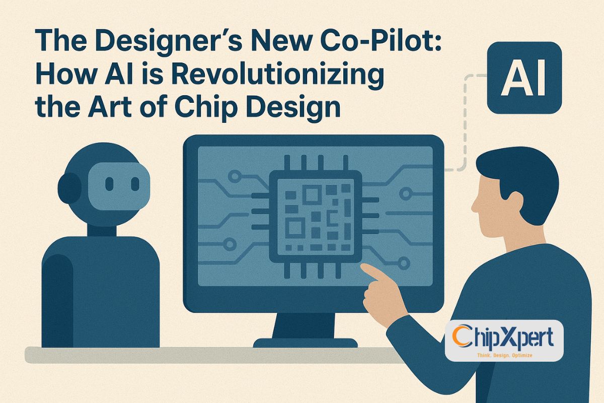
The Designer’s New Co-Pilot: How AI is Revolutionizing the Art of Chip Design
For decades, the process of designing a computer chip has been a monumental feat of human ingenuity. Imagine orchestrating a billion-piece orchestra on a speck of silicon, where every single transistor must be placed and connected with nanoscale precision. This task, known as placement and routing, is one of the most complex and time-consuming stages of chip design, handled by powerful but traditionally brute-force EDA (Electronic Design Automation) tools.
But we’re on the cusp of a seismic shift. What if the tools themselves could learn? What if they could suggest the optimal layout, predict problems before they happen, and tirelessly optimize for power and performance? This isn’t a future fantasy. AI and Machine Learning are now actively co-piloting the design of the next generation of chips.
From Brute Force to Brain Power
Traditional EDA software operates on a set of hard-coded rules. Engineers define the constraints (e.g., timing, power, area), and the software runs massive computations to find a solution that meets them. It’s effective, but it’s like using a super-powered calculator—it only does exactly what you tell it to, and exploring all possible solutions can take weeks or even months.
AI-infused EDA tools are different. They are trained on vast datasets from previous successful chip designs—terabytes of information on what worked, what didn’t, and why. By learning from this historical “collective wisdom,” ML models can:
- Predict Outcomes: Instead of running a full, slow simulation, an AI can quickly predict timing errors, signal integrity issues, or hot spots.
- Propose Optimizations: The AI can suggest innovative placement and routing solutions a human engineer might not have considered, breaking free from traditional design patterns.
- Explore the Design Space Rapidly: An AI can evaluate thousands of potential floorplans in the time it takes a traditional tool to evaluate a few dozen.
AI in Action: The Design Phase Revolution
So, what does this look like in the hands of an engineer? Let’s break it down:
1. Intelligent Placement:
Placing millions of logic gates is a mind-boggling puzzle. AI tools can now analyze the logical connectivity of a circuit (the netlist) and predict which blocks need to be placed close together to minimize wirelength and delay. It’s like having an assistant who instantly knows the perfect neighborhood for every component in a bustling city, reducing traffic jams (signal delays) from the start.
2. Smarter Routing:
Routing is the process of drawing the copper wires that connect all these placed components. AI can anticipate congestion hotspots—areas where too many wires are vying for space—and proactively route around them. This prevents a common, time-consuming problem where engineers have to go back and re-place components to fix unroutable areas. For those interested in the physical hardware these tools create, our guide on Understanding Semiconductor Packaging explains the final step in the journey.
3. Predictive Optimization:
Perhaps the most powerful application is prediction. ML models can now look at a preliminary design and accurately forecast its final performance, power consumption, and area (PPA). This allows engineers to make crucial trade-off decisions early in the design cycle, saving countless hours of late-stage re-spins. It’s like a weather forecast for your chip’s design, allowing you to pack an umbrella before it rains.
The Human-AI Partnership: Augmentation, Not Replacement
It’s crucial to understand that AI is not replacing chip designers. Instead, it’s automating the tedious, repetitive, and computationally brutal parts of the job. It frees up human engineers to do what they do best:
- Be Creative: Focus on high-level architecture and innovative circuit design.
- Make Strategic Decisions: Use the AI’s predictions and options to make informed choices about performance-power-area trade-offs.
- Solve Novel Problems: Tackle the unique challenges that AI, trained on past data, hasn’t encountered before.
This partnership makes the designer exponentially more productive, turning them from a detailed drafter into a strategic director.
The Ripple Effect: Why This Matters
The implications are profound. By drastically reducing the time and cost of design, AI is helping to keep Moore’s Law economically viable. It lowers the barrier to entry, allowing smaller companies and startups to innovate in the semiconductor space. Ultimately, it accelerates the pace of technological advancement for all of us, leading to faster, more efficient, and more specialized chips that will power everything from smarter phones to advanced medical devices.
The future of chip design isn’t about machines taking over. It’s about designers, armed with incredibly powerful AI co-pilots, reaching new heights of innovation that were previously unimaginable. The next breakthrough chip might not just be designed by a human, but with the collective intelligence of every chip that came before it.To see how industry leaders are implementing this technology, you can read about Synopsys’s AI-driven suite, DSO.ai, in this external article on IEEE Spectrum.
