Forget Monoliths: How Tiny Chiplets Are Building the Next Generation of Silicon
There’s a quiet revolution happening in the world of computer chips. For decades, the name of the game was making everything bigger, better, and—most importantly—on a single, flawless piece of silicon. These “monolithic” System-on-Chips (SoCs) are the brains inside your phone and laptop.
But we’re hitting a wall. As we demand more processing power, AI accelerators, and specialized cores, designing a single, gigantic chip is becoming astronomically expensive and complex. A tiny flaw anywhere in the design can render the entire chip useless.
So, what’s the answer? Think less like a sculptor carving a statue from a single block of marble, and more like a builder using LEGO bricks. The building blocks of the future are chiplets.
What Are Chiplets, Really?
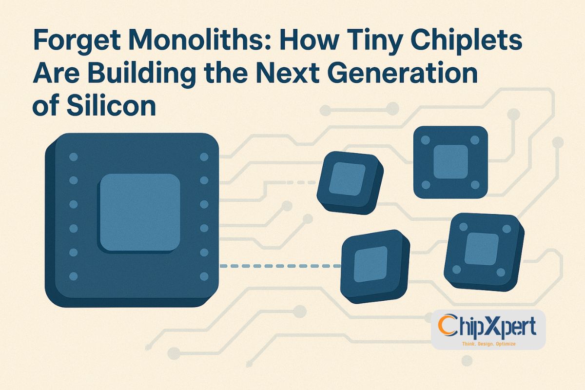
In simple terms, a chiplet is a small, modular piece of silicon that performs a specific function. Instead of building one massive chip, designers can create:
- A CPU chiplet (for raw processing power)
- A GPU chiplet (for graphics)
- An AI accelerator chiplet
- An I/O chiplet (for connectivity like USB or WiFi)
These individual chiplets are then connected and packaged together on a single substrate to act as one cohesive super-chip, or a “multi-die system.”
The benefits are huge. It’s cheaper, faster, and more sustainable to design and manufacture smaller, specialized blocks. You can mix and match the best “LEGO bricks” from different manufacturers, creating a custom processor tailored for a specific task. It’s a paradigm shift from “System-on-Chip” to “System-in-Package.”
The Magic Isn’t the Die, It’s the Handshake
The real genius of a chiplet-based system isn’t the chiplets themselves—it’s the incredibly high-speed communication between them. If they can’t talk to each other quickly and efficiently, the entire system falls apart. This is where Die-to-Die (D2D) interfaces come in.
Think of it like this: you could have the world’s best French chef, Italian pasta maker, and Japanese sushi chef. But if they’re stuck in separate kitchens with no way to communicate, you’ll never get a cohesive meal. Die-to-Die interfaces are the open-plan kitchen that lets them collaborate seamlessly.
These interfaces are the ultra-dense, ultra-fast wiring that allows data to flow between chiplets with minimal latency and energy use. They ensure that the group of chiplets performs as if they were a single, monolithic chip.
UCIe: The Universal Translator for Chiplets
For chiplets to truly work, we needed a standard. In the early days, every company had its own proprietary way of connecting its chiplets. It was like everyone speaking their own language—you couldn’t easily mix an Intel chiplet with one from AMD or TSMC.
Enter UCIe (Universal Chiplet Interconnect Express). Announced in 2022, UCIe is a groundbreaking open standard that aims to be the universal translator for the chiplet world.
UCIe defines everything needed for chiplets from different vendors to work together:
- The Physical Layer: The physical bumps, wires, and distances.
- The Protocol Layer: The “language” they speak (it leverages the popular PCI Express and Compute Express Link standards).
- The Software Stack: Ensuring the operating system recognizes it as one unit.
By creating this open ecosystem, UCIe unlocks true interoperability. It allows a company to buy a best-in-class AI chiplet from one vendor, a high-speed I/O chiplet from another, and pair it with their own CPU design. This fosters incredible innovation and specialization across the industry. For a deeper look at the physical packaging that makes this possible, check out our article on Understanding Semiconductor Packaging.
What This Means for You
This might all sound like inside baseball, but it has real-world impacts for all of us.
- Faster Innovation: Companies can design complex chips faster by reusing proven chiplet designs.
- Specialized Power: We’ll see processors optimized for specific tasks like gaming, AI, or data centers, built by combining the perfect set of chiplets.
- Cost Effectiveness: Eventually, this could lead to more powerful and efficient devices without the massive price hikes that following Moore’s Law alone would cause.
The age of the monolithic chip isn’t over, but the future is undoubtedly modular. Chiplets, connected by standards like UCIe, are building a more innovative, efficient, and powerful world of computing—one tiny, interconnected block at a time.To dive deeper into the technical specifications and the consortium behind it, you can read the official UCIe announcement on the AnandTech website.
