Complete Physical Design Flow in VLSI – From Netlist to GDSII
In the world of semiconductors, Physical Design is where theory meets tangible results. It’s the stage that bridges high-level RTL design to silicon-ready layout. For aspiring VLSI engineers and chip designers, understanding the complete Physical Design flow is essential for building efficient, low-power, and high-performance ICs.
This article breaks down the Physical Design process step by step — from netlist to GDSII — so you get a clear, beginner-to-pro level understanding of what really happens in the backend of chip design.
What is Physical Design in VLSI?
In simple terms, Physical Design is the process of transforming a synthesized netlist (a logical representation of the circuit) into a physical layout that can be fabricated on silicon.
While front-end design deals with logic (Verilog, SystemVerilog), physical design ensures that all those gates, flip-flops, and wires are placed correctly on the chip, taking into account real-world constraints like area, power, timing, signal integrity, and manufacturability.
If you’re looking to master the full flow hands-on, explore this Physical Design Course at ChipXpert
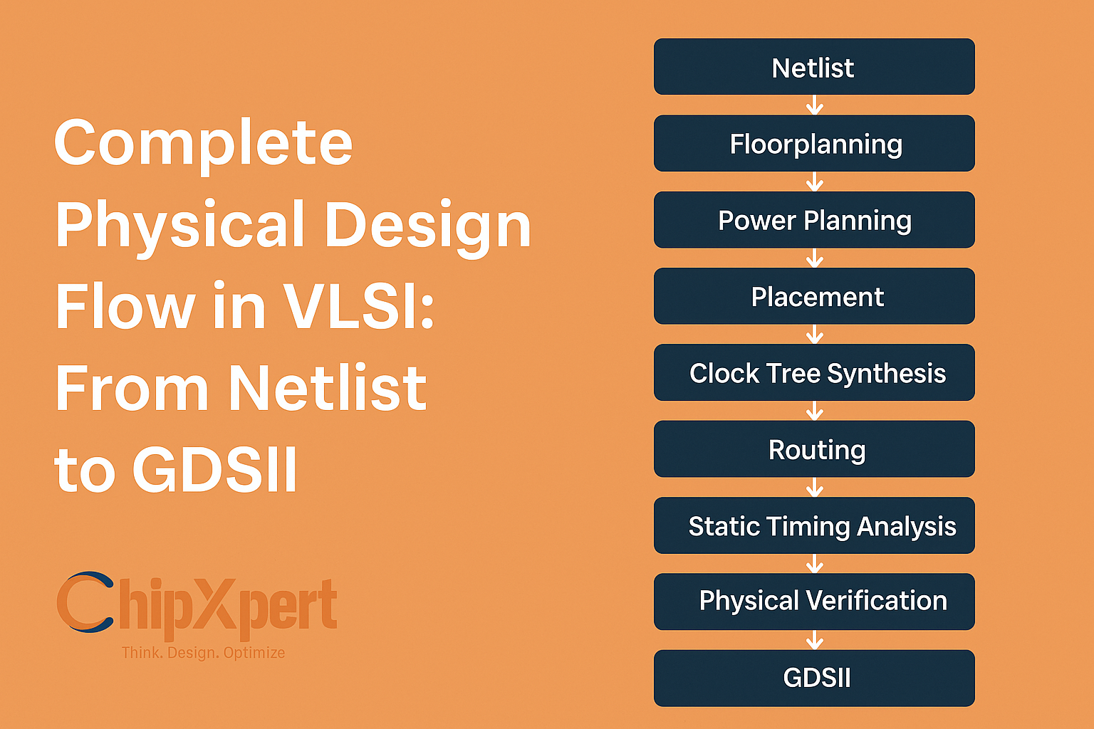
Step-by-Step Physical Design Flow
Let’s walk through each step of the standard ASIC Physical Design flow:
1. Importing Netlist and Design Constraints
After synthesis, the RTL code is converted into a gate-level netlist using standard cells. This netlist, along with timing constraints (SDC files), library files (LIB), and design specifications, is imported into the physical design tool (like Cadence Innovus or Synopsys ICC2).
At this stage, the design has no physical shape — it’s all logic. Your job is to bring it to life.
2. Floorplanning
This is the architectural foundation of your chip.
- Define core area and die size
- Place macros and hard IPs
- Reserve power/ground rings
- Create blockages for routing
Good floorplanning balances PPA (Power, Performance, Area). Think of it as placing furniture in a room for optimal movement and space usage.
3. Power Planning
You can’t run a circuit without a stable power network. In this step:
- Power rings and straps are designed
- Power grids are defined
- IR drop and electromigration (EM) considerations are analyzed
Power integrity is key. A bad power plan can result in chip failure.
4. Placement
Now it’s time to position your standard cells within the defined floorplan.
- Cells are placed logically to reduce wirelength and timing violations
- Congestion maps help identify routing bottlenecks
- Optimizations for timing, power, and density are applied
Placement heavily influences timing closure and routing effort later.
5. Clock Tree Synthesis (CTS)
This step is about distributing the clock signal to all sequential elements (flip-flops, latches) with minimal skew and latency.
- Clock buffers and inverters are inserted
- Clock tree is balanced using H-tree or other techniques
- Skew, insertion delay, and power are analyzed
CTS is critical for timing closure. A bad clock tree can lead to setup and hold violations.
6. Routing
Wires are now laid out to connect the logic cells and flip-flops.
- Global Routing gives a rough path
- Detailed Routing assigns exact metal layers and tracks
- Design Rule Checks (DRC) ensure spacing, width, and via rules are followed
Routing tools use advanced algorithms to avoid crosstalk, delay, and congestion.
7. Static Timing Analysis (STA)
Once routing is done, it’s time to verify if the chip meets timing specs.
- Tools like PrimeTime perform STA
- Setup and Hold violations are identified
- Paths are optimized using buffer insertion, gate sizing, and re-routing
Timing closure is often iterative — you fix violations, rerun analysis, and repeat until success.
8. Physical Verification: DRC and LVS
You’re almost at the finish line — but you need to verify that the layout is manufacturable and correct.
- DRC (Design Rule Check) ensures the layout follows foundry rules
- LVS (Layout vs Schematic) ensures the netlist matches the layout
- Antenna effects, ERC, and Metal fill rules are also checked
Tools like Calibre (Mentor) or IC Validator (Synopsys) are industry standards here.
9. Antenna Checks and ECOs
During fabrication, certain nets may accumulate charge (antenna effect) and damage transistors.
- Add antenna diodes or metal jumps
- Perform Engineering Change Orders (ECOs) if needed to fix bugs without full re-run
This step ensures yield and reliability of the chip.
10. GDSII Generation and Tape-Out
The final step. The verified layout is converted into a GDSII (Graphic Database System II) file — the format sent to the foundry for mask generation and fabrication.
This is called tape-out, a big milestone in any chip project.
Tools Used in Physical Design
Here’s a snapshot of industry-standard tools:
| Task | Tool Examples |
|---|---|
| Floorplanning & Place | Cadence Innovus, Synopsys ICC2 |
| CTS | Cadence Tempus, PrimeTime |
| Routing | ICC2, Innovus |
| STA | Synopsys PrimeTime |
| DRC/LVS | Mentor Calibre, Synopsys ICV |
Learning and gaining hands-on experience in these tools is a huge advantage.
Why Physical Design is a High-Impact Career
- In-demand skill with increasing chip complexity
- High-paying jobs in India and abroad
- Direct involvement in real-world semiconductor innovation
- Clear career ladder: Junior → Lead → Manager → Architect
Further Reading and Industry Resources
If you’d like to deep-dive into recent developments in Physical Design, check out:
Final Thoughts
Physical Design isn’t just about placing cells or running scripts — it’s about realizing an idea in silicon. Every step, from floorplanning to GDSII, demands precision, engineering intuition, and continuous learning.
If you’re passionate about building the chips that power the future, mastering Physical Design is your launchpad. Whether you’re a student or a professional, understanding this flow deeply will empower you to contribute to billion-transistor SoCs and cutting-edge technologies.
