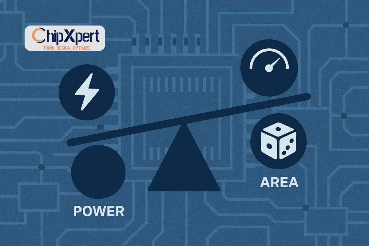
The PPA Triad in the Angstrom Era: A High-Stakes Balancing Act at 3nm and Below
For decades, the goal of every chip designer has been elegantly summarized by three letters: PPA.
- Power: How much energy does it consume?
- Performance: How fast can it compute?
- Area: How small is the silicon die?
Achieving the right balance of these three metrics has always been the core challenge. But as we cross the threshold from nanometers into the angstrom era (1nm = 10 angstroms), the rules of the game have changed dramatically. At process nodes of 3nm, 2nm, and beyond, optimizing for PPA is no longer just a design challenge, it’s a high-stakes physics problem.
At ChipXpert, we prepare the next generation of VLSI engineers for this reality. The strategies that worked at 28nm or even 7nm are no longer sufficient. Let’s break down why PPA optimization is harder than ever and what tools and techniques are emerging to master this new triad.
Why the Angstrom Era Breaks Old Rules
The problems at these advanced nodes are fundamental:
- Physics Gets “Weird”: Quantum effects like tunneling and variability become dominant. Transistors don’t just turn on and off cleanly; electrons can teleport through barriers, leading to significant leakage power even when the chip is idle. This directly undermines the ‘Power’ in PPA.
- The Interconnect Crisis: While transistors have gotten smaller, the copper wires connecting them haven’t scaled as effectively. Their resistance has skyrocketed, causing RC delay and becoming a major bottleneck for ‘Performance’. The wires now often dominate power consumption and timing.
- Prohibitively High Costs: The cost of a single mask set and fabrication run at 3nm is astronomical. This magnifies the importance of ‘Area’. Every square micron saved translates to millions of dollars saved in production and higher yield. There is zero room for error.
The Modern PPA Optimization Toolkit
Surviving in the angstrom era requires a new arsenal of advanced strategies that work together from architecture to implementation.
1. Architectural-Level Strategies: The Biggest Levers
The most significant PPA wins happen before a single line of RTL is written.
- Hardware Specialization: The era of the one-size-fits-all CPU is over. The biggest performance-per-watt gains come from Domain-Specific Architectures (DSAs)—dedicated accelerators for AI, graphics, encryption, etc. These hardware blocks are orders of magnitude more efficient for their specific task than a general-purpose processor.
- Advanced Memory Hierarchies: Managing data movement is critical for power. Architects are employing complex, multi-level memory systems and techniques like Near-Memory Computing to minimize the energy-costly movement of data across the chip.
- Fine-Grain Power Management: This goes beyond simple sleep modes. Techniques like Dynamic Voltage and Frequency Scaling (DVFS) and Adaptive Voltage Scaling (AVS) allow different blocks on the chip to run at their minimum required voltage and frequency, drastically saving power.
2. RTL and Implementation-Level Strategies
This is where the architect’s vision meets the silicon.
- Multi-Vt Cell Optimization: Using a mix of standard cells with different threshold voltages (Low-Vt for speed-critical paths, High-Vt to reduce leakage everywhere else) is a classic technique that is now absolutely essential.
- Use-Based Optimization: Tools can now automatically identify and downsize over-designed cells (e.g., a large driver where a small one would suffice) or clone large fan-out buffers to improve timing without a power penalty.
- Advanced Floorplanning: With interconnect delay so costly, physical proximity is critical. Tightly coupling related blocks and macros (a practice often called “physically aware design“) is crucial to meet performance targets.
3. The Foundry-Designer Partnership: DTCO and STCO
You can no longer design in a vacuum. PPA optimization is now a continuous dialogue between the designer and the foundry.
- DTCO (Design Technology Co-Optimization): Foundries now offer a portfolio of cells and architectures (e.g., different standard cell heights, backside power delivery like Intel’s PowerVia) for a single node. Designers must choose the right options for their specific PPA targets.
- STCO (System Technology Co-Optimization): This takes it a step further, considering how the package, die, and memory will work together as a system. Using 2.5D/3D integration and chiplets is a direct result of STCO, allowing designers to use the optimal node for each function (e.g., 3nm for compute, 12nm for I/O) to achieve the best system-level PPA.
What This Means for the VLSI Engineer
The role of the VLSI engineer is evolving. It’s no longer enough to be an expert in a single domain like RTL design or physical design. The most valuable engineers are those who understand the entire flow—from architecture and system-level trade-offs down to the physics of the transistor.
They are engineers who can speak the language of:
- Architects to understand the power and performance intent.
- Physical Designers to implement that intent under extreme constraints.
- Tool Experts to leverage the full capabilities of complex EDA suites.
Learn the Art of PPA at ChipXpert
Mastering the PPA triad in the angstrom era is the defining challenge for today’s chip designers. It requires a deep, integrated understanding of concepts that span across multiple domains.
At ChipXpert, our advanced curriculum is designed to provide this holistic view. We don’t just teach tools; we teach the underlying principles and trade-offs that empower you to make intelligent PPA decisions.
Ready to tackle the high-stakes challenges of advanced-node design? Explore our comprehensive VLSI courses and learn the art and science of PPA optimization from industry experts.


