
Understanding the ASIC Design Flow: Key Steps Explained for Aspiring Engineers
The world of VLSI (Very Large Scale Integration) design is both exciting and complex, offering immense opportunities for engineers looking to shape the future of technology. At ChipXpert VLSI Training Institute, we aim to demystify the ASIC (Application-Specific Integrated Circuit) design flow to empower aspiring engineers with the knowledge and skills needed to excel in this dynamic field. Whether you’re a recent graduate or a professional seeking to enhance your expertise, understanding the ASIC design process is a critical step toward a rewarding career in semiconductor design. In this blog, we’ll explore the key stages of the ASIC design flow, optimized for clarity and engagement, while ensuring you’re equipped to take your first steps in VLSI with confidence.
What is ASIC Design?
ASICs are custom-designed integrated circuits tailored for specific applications, such as smartphones, medical devices, or automotive systems. Unlike general-purpose chips, ASICs are optimized for performance, power efficiency, and cost, making them a cornerstone of modern electronics. The ASIC design flow is a structured process that transforms a concept into a functional, manufacturable chip. At ChipXpert, our comprehensive ASIC Physical Design Course guides students through each phase, blending theory with hands-on practice.
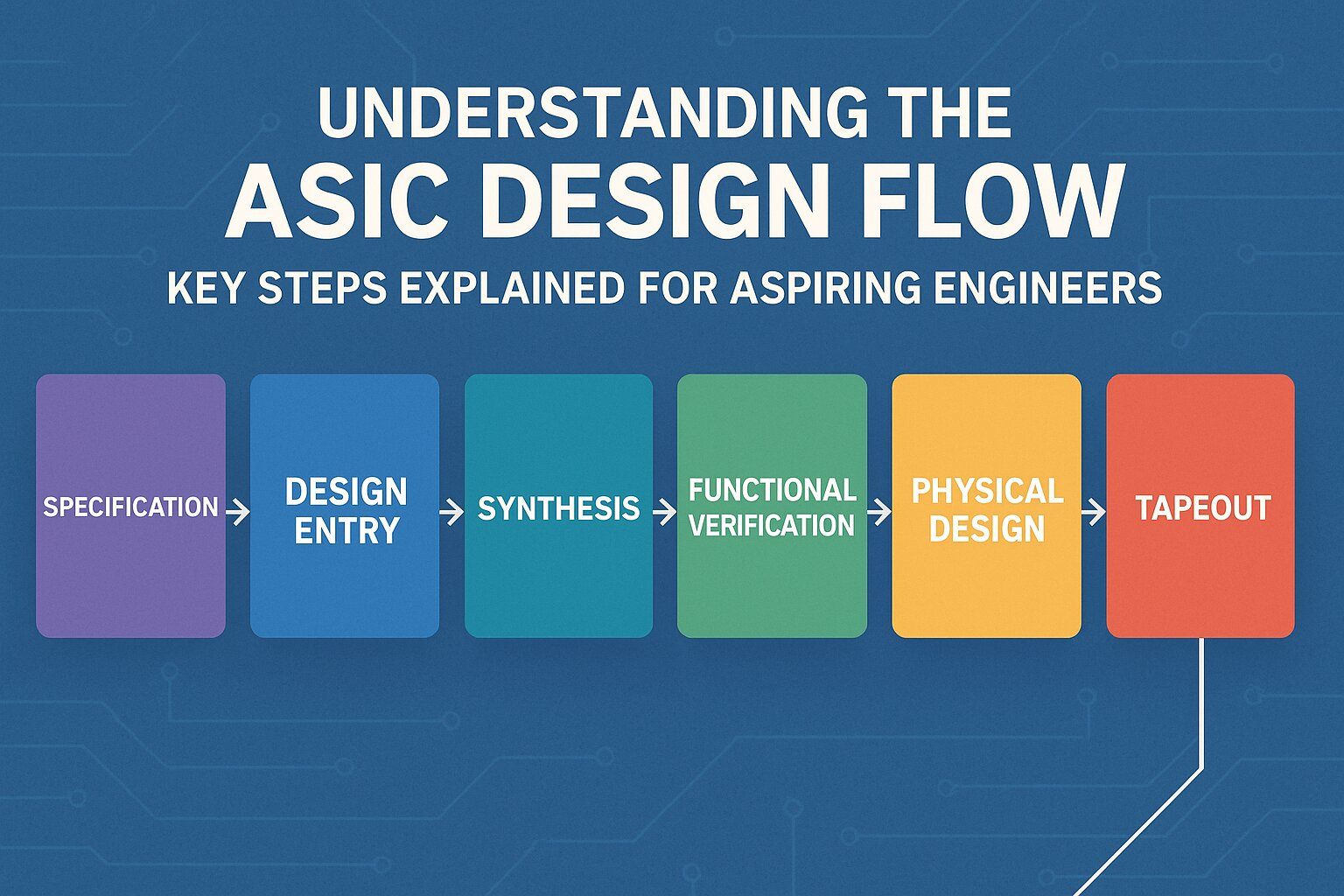
Key Steps in the ASIC Design Flow
The ASIC design flow is a multi-stage process that requires precision and expertise. Below, we break down the essential steps, offering insights into their significance and how they contribute to creating high-performance chips.
1. Specification and Architecture Design
Every ASIC begins with a clear design specification, which outlines the chip’s functionality, performance goals, and constraints like power and area. This phase involves collaboration between engineers and stakeholders to define requirements, such as processing speed or compatibility with other systems. The architecture design then translates these specifications into a high-level blueprint, determining the chip’s structure and key components.
At ChipXpert, our training emphasizes real-world specification development, ensuring students understand how to align design goals with industry needs. For more insights into chip architecture, check out this guide on VLSI design basics from Synopsys.
2. RTL Design and Verification
The next step is Register Transfer Level (RTL) design, where the chip’s functionality is described using hardware description languages like Verilog or VHDL. This code defines how data moves between registers and logical operations. Verification ensures the RTL code meets the specified requirements through simulations and testbenches.
Our Verilog training module at ChipXpert equips students with practical skills to write and verify RTL code, preparing them for industry-standard tools like ModelSim. Learn more about RTL verification from this resource on functional verification by Cadence.
3. Synthesis
During synthesis, the RTL code is transformed into a gate-level netlist, a representation of the design using standard cells (logic gates). This process involves optimizing the design for timing, power, and area using tools like Synopsys Design Compiler. Engineers also define timing constraints in SDC (Synopsys Design Constraints) format to ensure the design meets performance goals.
ChipXpert’s curriculum includes hands-on synthesis labs, teaching students how to analyze synthesis reports and optimize designs. For a deeper dive into synthesis, explore this overview of logic synthesis from Siemens EDA.
4. Floorplanning
Floorplanning is the first step in physical design, where engineers plan the chip’s layout. This includes estimating die size, placing I/O pads, and positioning macros (like memory blocks or PLLs) to minimize wirelength and congestion. A well-executed floorplan ensures efficient use of chip area and supports power and signal integrity.
Our ASIC Physical Design Course covers floorplanning techniques, including die size estimation and macro placement strategies, using tools like Cadence Innovus. For more on floorplanning, refer to this detailed guide from EE Times.
5. Power Planning
A robust power delivery network (PDN) is critical for chip reliability. Power planning involves designing power rings, straps, and rails to distribute power evenly across the chip while minimizing voltage drops. This step ensures the chip operates efficiently without power-related failures.
At ChipIndustry standards, such as those outlined by IEEE, guide power planning, and our courses teach students how to implement these using industry tools.
6. Placement
In the placement phase, standard cells and macros are arranged on the chip to optimize performance, routability, and power efficiency. Engineers insert end-cap cells, tap cells, and I/O buffers to prevent design rule violations and perform timing analysis to ensure setup and hold times are met.
ChipXpert’s training includes placement optimization techniques, such as congestion analysis and high-fanout net synthesis, preparing students for real-world challenges. Learn more about placement strategies in this technical article from Semiconductor Engineering.
7. Clock Tree Synthesis (CTS)
Clock Tree Synthesis ensures a balanced clock distribution network to minimize skew and latency. This step is crucial for synchronizing the chip’s operations. Engineers also perform scan chain reordering to optimize testability and reduce routing overhead.
Our hands-on CTS labs at ChipXpert use tools like Synopsys IC Compiler to teach students how to build efficient clock trees. For further reading, check out this CTS tutorial from Analog Devices.
8. Routing
Routing connects the placed cells and macros using metal layers, ensuring signal integrity and minimal congestion. Engineers analyze routing to avoid violations and optimize for performance. This step also includes power routing to maintain a reliable PDN.
ChipXpert’s curriculum covers routing techniques, including channel-width estimation and congestion management, using tools like Cadence Encounter. Explore routing challenges in this article on physical design from Design & Reuse.
9. Static Timing Analysis (STA) and Physical Verification
Static Timing Analysis (STA) verifies that the design meets timing requirements, checking for setup and hold violations. Physical verification ensures the layout adheres to manufacturing rules, using checks like DRC (Design Rule Check) and LVS (Layout vs. Schematic).
Our STA training at ChipXpert provides in-depth knowledge of timing analysis and verification, preparing students for sign-off processes. For more on STA, see this guide from Synopsys.
10. Sign-Off and Fabrication
The final step is sign-off, where the design is validated for functionality, timing, and manufacturability. The verified layout is sent to the foundry for fabrication, resulting in a physical chip ready for testing and deployment.
ChipXpert’s industry-aligned training ensures students are ready to navigate this critical phase, with exposure to tools like Mentor Graphics Calibre.
Why Learn ASIC Design at ChipXpert?
At ChipXpert VLSI Training Institute, we bridge the gap between academic theory and industry practice. Our courses, offered both online and offline in Hyderabad, cover the entire ASIC design flow, from RTL design to physical verification. With expert instructors, hands-on labs, and access to industry-standard tools, we prepare students for roles at top semiconductor companies like Intel, Qualcomm, and TSMC.
Our ASIC Physical Design Course includes:
- Training in Verilog, synthesis, and physical design tools
- Real-world projects to build a strong portfolio
- Career guidance and placement support
For additional resources, explore VLSI Design Tutorials for practical insights into chip design.
Conclusion
Mastering the ASIC design flow is a gateway to a thriving career in VLSI. From specification to fabrication, each step requires precision, creativity, and technical expertise. At ChipXpert, we’re committed to helping aspiring engineers navigate this complex process with confidence. Whether you’re starting your journey or advancing your skills, our tailored training programs provide the tools and knowledge to succeed.
Ready to dive into the world of ASIC design? Enroll in our ASIC Physical Design Course today and take the first step toward a rewarding career in VLSI!
