The Analog Art Form Meets Digital Physics: Layout in the FinFET and GAA Era
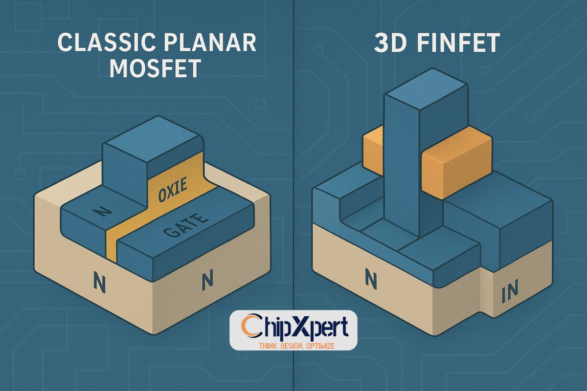
For analog layout engineers, the canvas has always been silicon. Their artistry—meticulously matching transistors, shielding sensitive lines, and crafting patterns that are both precise and manufacturable—has long been the backbone of mixed-signal chips. But the canvas has changed. The gentle slopes of planar transistors have been replaced by the sharp, three-dimensional cliffs of FinFETs and Gate-All-Around (GAA) transistors.
This shift, which delivered monumental gains for digital logic, has turned analog layout on its head. The old rules no longer apply. At ChipXpert, we train engineers to not just adapt to this new reality but to master it. Let’s explore the profound challenges and new techniques defining analog layout in the advanced-node era.
Why Analog Layout is Harder on a 3D Canvas
Digital design automated. Analog design remained manual, relying on intuition and well-understood rules. FinFETs and GAA transistors introduce quantum effects and complex 3D geometries that break that intuition.
Challenge 1: The Device Matching Nightmare
Matching identical transistors is the absolute foundation of analog design (e.g., in differential pairs, current mirrors). At advanced nodes, this becomes incredibly difficult.
- The Problem: The electrical characteristics of a FinFET are exquisitely sensitive to its physical environment. Stress from nearby features, line edge roughness (LER), and quantum confinement effects in the fin all contribute to variability. Two transistors that look identical in the layout can behave very differently.
- New Techniques:
- Context-Aware Placement: It’s no longer enough to place devices close and with the same orientation. Layout engineers must now consider the dummy fin requirements and the stressors placed by the digital standard cells surrounding the analog block. A mismatch in the local environment can cause a mismatch in performance.
- Larger Area, More Fins: To average out random variations, designers often need to use larger devices with more fins, trading off precious area for the necessary matching precision.
Challenge 2: The Parasitic Extraction Black Box
In the planar era, engineers could often “eyeball” parasitic capacitance and resistance. In the FinFET era, it’s a guessing game.
- The Problem: The 3D structure of a FinFET creates complex, multi-dimensional parasitic capacitors. Capacitance no longer exists just between wires; it exists between the gate, fin, source, and drain in ways that are nearly impossible to intuit. Resistance is equally complex, depending on the number of fins, contact placement, and local silicide blocking.
- New Techniques:
- Total Reliance on EDA: Analog designers must now place a transistor and then run a parasitic extraction to even understand its basic performance. The layout-simulation loop becomes much tighter and more iterative.
- Post-Layout Simulation is Mandatory: Pre-layout simulation results are mere estimates. Sign-off requires post-layout simulation with extracted parasitics to ensure the circuit will actually work. This adds significant time to the design cycle.
Challenge 3: Design for Manufacturing (DFM) on Steroids
The rules for making a chip manufacturable have become exponentially more complex.
- The Problem: FinFET fabrication requires a host of new patterning techniques like Multi-Patterning (LELE, SADP) and EUV. This introduces new layout-dependent errors and restrictions.
- Dummy Features: The requirement for dummy fins and dummy gates to ensure uniform etching and polishing means the final fabricated structure looks different from what the designer drew.
- Stress and Well Proximity Effects: The mechanical stress imposed by shallow trench isolation (STI) and well boundaries drastically alters carrier mobility. Placing a transistor too close to a well boundary can change its threshold voltage (Vt).
- New Techniques:
- DFM Audits are Critical: Running automated DFM checks throughout the layout process is non-negotiable. Engineers must check for forbidden pitches, multi-patterning conflicts, and density violations.
- Collaboration with Foundries: Successful analog layout requires constant dialogue with the foundry to understand their specific DFM rules and recommendations, which can change from node to node.
The Tooling Evolution: EDA to the Rescue (Mostly)
The industry is responding with more analog-aware tools, but the human touch remains vital.
- FinFET-Aware Analog Planners: Tools are emerging that can help plan analog blocks while automatically adhering to fin grid and multi-patterning rules.
- Advanced Extraction: Field solvers are becoming more integrated to provide accurate parasitic estimates earlier in the flow.
- Machine Learning: ML is being explored to predict the impact of layout choices on performance and variability, potentially guiding designers toward more optimal and robust layouts.
What This Means for the Analog Layout Engineer
The job description has evolved. The modern analog layout engineer must be:
- A Physicist: Understanding the underlying device physics that govern FinFET behavior.
- A DFM Expert: Intimately knowing the complex manufacturing rules and how to avoid their pitfalls.
- An EDA Power User: Leveraging advanced tools for extraction and analysis at every step.
- A Digital Liaison: Understanding the impact of the surrounding digital logic on their sensitive analog blocks.
Master the New Analog Reality at ChipXpert
The transition to FinFET and GAA has made analog layout more challenging, but also more critical than ever. The need for expertly crafted analog interfaces in a digital world is only growing.
At ChipXpert, our Analog Layout training program is specifically designed to address this new reality. We go beyond the basics to teach the advanced techniques, tool flows, and physics-aware strategies needed to succeed at the most advanced nodes.
Ready to master the art of analog layout on a 3D canvas? Explore our Analog Layout training program and learn how to design robust, high-performance circuits in the FinFET and GAA era.


