

What Is Clock Tree Synthesis (CTS)?
Clock tree synthesis is the physical-design step that builds the network delivering the clock from its source to every sequential element in the design. Before CTS the clock is an ideal, zero-delay signal in the timing model. After CTS it is real: buffered, routed, and carrying genuine latency and skew. The job of CTS is to make that real network arrive everywhere close enough to simultaneously that setup and hold can both be met.
The Classical Clock Tree Architectures
- H-tree: a recursively branching, geometrically symmetric structure. Every leaf sits at an identical path length from the root, so skew is minimal by construction. It is elegant and predictable, but it ignores where the flops actually are and consumes significant routing resource.
- Clock mesh (grid): a grid of clock wire driven from many points and shorted together. Shorting averages out variation, giving excellent skew and jitter tolerance, at the cost of high capacitance and therefore high clock power. Used where skew matters more than power — high-performance CPUs.
- Buffered tree / fishbone: the pragmatic default. A spine feeds branch buffers that fan out to local flop clusters. It follows the real placement, so it costs far less power than a mesh, and modern tools balance it algorithmically rather than geometrically.
- Multi-source CTS: a hybrid — a mesh or spine at the top level feeding conventional trees locally. This is the structure most advanced-node designs converge on, and it is covered in depth below.
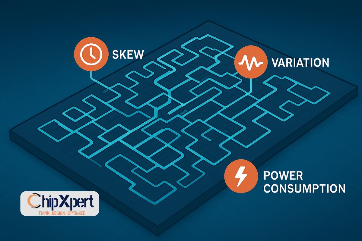
The choice is a three-way trade between skew, power and routing area. No architecture wins outright; the correct one depends on the clock frequency, the flop count, and how much power budget the clock network is allowed to consume — often 30% or more of total dynamic power.
In the world of chip design, the clock signal is the conductor of the orchestra. It dictates the precise rhythm for every sequential element, ensuring billions of transistors dance in perfect synchrony. Getting this timing right is the job of Clock Tree Synthesis (CTS), a critical step in the physical design flow.
For years, CTS was a relatively standardized process. But at advanced nodes—3nm, 2nm, and into the angstrom era—the rules of the game have changed entirely. What was once a challenging but manageable task has become one of the most complex and critical hurdles to achieving timing closure.
At ChipXpert, we ensure our students are prepared for the industry’s toughest challenges. Let’s break down why CTS is so difficult at the edge of Moore’s Law and how engineers are developing new strategies to tame this beast.
Why CTS is a Nightmare at Advanced Nodes
The problems are fundamental and interconnected:
- The Variability Volcano: At 3nm and below, microscopic variations in the manufacturing process become significant. Differences in transistor threshold voltage (Vt), channel length, and oxide thickness are no longer statistical noise; they are dominant forces. This process variation means two identical clock buffers placed next to each other can have slightly different delays, instantly creating clock skew.
- The Interconnect Dominance: Resistance in the tiny copper wires has skyrocketed. This means the delay of the clock path is no longer primarily determined by the buffers but by the RC delay of the wires themselves. Predicting and controlling this is incredibly difficult, making skew minimization a moving target.
- The Power Beast: The clock network is typically the largest single net on the chip and can consume 25-40% of total dynamic power. At advanced nodes, controlling this power is non-negotiable. Every buffer added to balance skew adds to this power burden, creating a tightrope walk between timing and power.
- The Congestion Crisis: Advanced nodes pack an astronomical number of cells into a small area. Finding physical space to route a robust, balanced clock tree without creating routing congestion is a major challenge. Congestion itself can lead to longer, more resistive wires, further exacerbating skew and delay problems.
The Consequences of a Poor Clock Tree
A poorly synthesized clock tree doesn’t just mean a slower chip; it can lead to catastrophic failure:
- Hold Violations: Excessive clock skew can cause a signal to arrive too quickly at a capture flip-flop, violating hold time and creating a functional failure that is often irreparable after fabrication.
- Setup Violations: Global clock latency eats into the time available for data to compute, limiting the maximum operating frequency (performance) of the chip.
- Clock Gating Issues: Implementing power-saving clock gating becomes riskier, as glitches or timing errors on the gating logic can shut down the clock for entire sectors erroneously.
Advanced Strategies to Tame Modern CTS
Thankfully, the EDA industry and design methodologies are evolving to meet these challenges. Taming the clock tree now requires a multi-pronged approach:
1. Useful Skew and Clock Tree Optimization
The old goal was “zero skew.” The new goal is “controlled useful skew.” Advanced CTS tools can now intentionally introduce skew to help fix setup and hold violations. By carefully delaying the clock to certain registers, designers can effectively borrow time from one path to give to another. This requires sophisticated, signoff-aware analysis throughout the flow.
2. Multi-Source CTS (MS-CTS) and Clustering
Instead of building a single, monolithic tree from one root, MS-CTS creates multiple local clock trees driven by regional roots. This reduces the overall latency and the load on any single driver, making the tree more resilient to variation and easier to balance locally. This is often combined with register clustering, where flip-flops are placed physically close to their clock source.
3. Advanced On-Chip Variation (AOCV) Modeling
Using traditional derating factors is too pessimistic at advanced nodes. AOCV provides more nuanced, context-aware derating tables based on a cell’s location and logic depth. This reduces over-design and allows for a more accurate and less conservative clock tree, improving PPA.
4. Clock Gate Cloning and Placement
A large clock gate feeding thousands of registers creates a huge load and a single point of failure. The solution is to clone the clock gate—creating several identical instances—and strategically place them across the design to drive local regions. This reduces load, minimizes insertion delay, and improves the clock gating structure’s robustness.
5. The Rise of AI/ML in CTS
Machine Learning is now being applied to predict routing congestion and RC parasitics before CTS is run. This allows the tool to build a clock tree that is inherently resilient to these effects. AI can also help optimize the complex trade-off between power, skew, and latency, finding solutions that traditional algorithms might miss.
What This Means for the Physical Design Engineer
The role of the physical design engineer has evolved.成功实施CTS不再仅仅是运行一个工具。它需要:
- A Deep Understanding of Variation: Engineers must think statistically, not just deterministically.
- Mastery of Advanced Tool Flows: Knowing how to set up and interpret AOCV, useful skew, and MS-CTS is now a required skill.
- A Holistic View of PPA: Every decision in CTS has a ripple effect on timing, power, and area. The engineer must constantly balance these competing constraints.
Master Modern CTS at ChipXpert
Clock Tree Synthesis is a microcosm of the broader challenges in advanced-node design: mastering complexity, embracing new methodologies, and leveraging powerful tools.
At ChipXpert, our advanced Physical Design training curriculum places a strong emphasis on these critical, industry-relevant skills. We don’t just teach the basics; we dive deep into the strategies and tools needed to achieve closure on the most complex modern designs.
Ready to conquer the clock and master advanced-node physical design? Explore our Physical Design training program and learn the art and science of taming timing closure from industry experts.
Share your question in comments or talk to our mentor team for batch guidance.
Ask the Admin Team
Drop your basic question in comments: eligibility, prerequisites, tools, fee range, and placement support.
Our team reviews and responds regularly.