As semiconductor devices shrink to nanometer dimensions, engineers encounter phenomena that are rarely observed in everyday electronics. One of the most fascinating is Quantum Tunneling a quantum mechanical effect that allows electrons to pass through barriers that would be impossible to cross under classical physics. While this phenomenon enables innovative technologies, it also creates significant challenges for modern chip design.
What Is Quantum Tunneling?
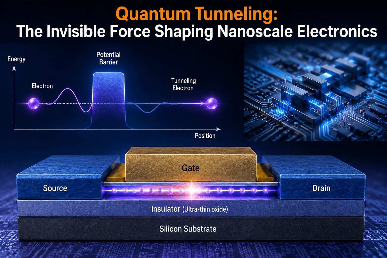
In classical physics, an electron must possess enough energy to overcome a barrier. Quantum mechanics, however, introduces a different possibility.
Quantum tunneling occurs when an electron has a probability of passing through an energy barrier even when it lacks the energy required to cross it directly. At nanoscale dimensions, where transistor features are only a few nanometers wide, this effect becomes increasingly significant.
Simply put, electrons can tunnel through barriers instead of going over them.
Why Does Quantum Tunneling Matter in Modern Chips?
As semiconductor manufacturers continue to scale transistors to smaller nodes, gate oxides and device dimensions become extremely thin.
This creates new challenges:
- Increased leakage current
- Higher standby power consumption
- Reduced device reliability
- Greater heat generation
- Difficulty maintaining transistor control
What was once a negligible effect has become a major consideration in advanced semiconductor design.
Types of Quantum Tunneling in Semiconductor Devices
Several forms of tunneling are commonly observed in nanoscale devices:
Gate Oxide Tunneling
Electrons tunnel through the ultra-thin gate dielectric, causing leakage currents.
Direct Tunneling
Occurs when electrons pass directly through very thin insulating layers.
Fowler-Nordheim Tunneling
Takes place under strong electric fields and is widely used in flash memory technologies.
Band-to-Band Tunneling
Electrons move directly between energy bands, contributing to leakage in advanced transistors.
Each type affects device behavior differently and requires careful engineering control.
The Impact on Nanoscale Transistors
Quantum tunneling directly influences transistor performance as technology nodes continue to shrink.
Key impacts include:
- Increased static power dissipation
- Lower battery life in portable devices
- Reduced switching efficiency
- Greater thermal management challenges
- Performance variability across devices
Managing these effects has become one of the most critical challenges in semiconductor scaling.
Engineering Solutions to Control Tunneling
To minimize unwanted tunneling effects, semiconductor manufacturers employ several advanced techniques:
High-k Dielectrics
Materials with higher dielectric constants provide better insulation while maintaining electrical performance.
FinFET and GAAFET Architectures
Advanced transistor structures improve gate control and reduce leakage currents.
Material Innovation
New semiconductor materials help optimize electron behavior at nanoscale dimensions.
Optimized Device Design
Engineers carefully balance performance, power, and reliability through innovative device architectures.
These solutions allow continued scaling while keeping tunneling effects under control.
Quantum Tunneling: Challenge and Opportunity
Although tunneling creates design challenges, it also enables several breakthrough technologies:
- Flash memory storage
- Tunnel Field-Effect Transistors (TFETs)
- Quantum computing devices
- Nanoscale sensors
- Advanced memory technologies
Researchers are increasingly exploring ways to harness tunneling rather than simply suppress it.
Conclusion
Quantum tunneling demonstrates how semiconductor engineering enters a fundamentally different world at nanometer scales. As transistors become smaller, understanding and controlling electron behavior is essential for maintaining performance and efficiency. While tunneling introduces new design challenges, it also opens the door to innovative technologies that could define the future of computing.
Share your question in comments or talk to our mentor team for batch guidance.
Ask the Admin Team
Drop your basic question in comments: eligibility, prerequisites, tools, fee range, and placement support.
Our team reviews and responds regularly.
