For decades, the semiconductor industry has focused on making transistors smaller, faster, and more power-efficient. Moore’s Law enabled the integration of billions of transistors onto a single chip, driving incredible advances in computing performance. However, as technology nodes continue to shrink toward 2nm and beyond, a surprising reality is emerging:
Transistors are no longer the primary bottleneck in chip performance. Interconnects are.
Modern processors contain tens of billions of transistors, but the ability of these transistors to communicate efficiently has become one of the biggest challenges in semiconductor design. Today, the wires connecting transistors often consume more power, introduce more delay, and create more design complexity than the transistors themselves.
Understanding Interconnects: The Nervous System of a Chip
Interconnects are the microscopic metal wires that connect transistors and functional blocks inside a semiconductor device.
Just as neurons connect different parts of the human brain, interconnects allow information to travel between:
- CPU cores
- Cache memories
- AI accelerators
- Memory controllers
- Input/Output interfaces
Without interconnects, billions of transistors would simply operate as isolated devices with no way to exchange data.
Modern high-performance processors may contain several kilometers of metal wiring when all routing layers are combined and scaled to real-world dimensions.
As chips become larger and more complex, interconnect networks become increasingly critical to overall system performance.
The Shift from Transistor Bottlenecks to Interconnect Bottlenecks
Historically, transistor switching speed limited processor performance.
As manufacturing technologies evolved:
- Transistors became smaller.
- Switching speeds improved dramatically.
- Power efficiency increased.
However, interconnect scaling did not improve at the same pace.
While transistor dimensions shrank, wire resistance increased because metal lines became narrower and thinner. At the same time, capacitance between adjacent wires remained significant.
As a result:
- Signal propagation delays increased.
- Power losses became larger.
- Communication between blocks became slower.
Today, moving data across a chip often consumes more time and energy than performing the actual computation.
This phenomenon is known as the Interconnect Bottleneck.
Why Data Movement Is Becoming the Real Challenge
In modern computing systems, processing data is relatively inexpensive compared to moving it.
Consider an AI accelerator:
- A mathematical operation may require only a small amount of energy.
- Retrieving data from memory can consume significantly more energy.
- Transporting data across long interconnect paths adds additional delay and power consumption.
For advanced AI workloads:
- Data movement can account for more than half of total energy consumption.
- Memory access often dominates execution time.
- Communication overhead limits system scalability.
This is why semiconductor companies are increasingly focusing on reducing data movement rather than simply increasing transistor counts.
The industry is discovering that faster computation alone is not enough if data cannot reach the processing units efficiently.
Challenges Facing Modern Interconnects
Resistance and Capacitance
As metal wires become smaller:
- Electrical resistance increases.
- Signal degradation becomes more severe.
- Delays increase significantly.
Routing Congestion
Modern chips contain billions of interconnected components.
Challenges include:
- Limited routing resources.
- Complex signal paths.
- Increased design difficulty.
Power Consumption
Interconnects contribute substantially to overall chip power.
Key issues include:
- Dynamic switching power.
- Leakage currents.
- Voltage drops across power networks.
Thermal Effects
Dense routing layers generate heat and create hotspots.
This can affect:
- Performance
- Reliability
- Long-term device lifespan
These challenges become more severe with every new technology node.
Industry Solutions to the Interconnect Problem
Semiconductor companies are investing heavily in new technologies to overcome interconnect limitations.
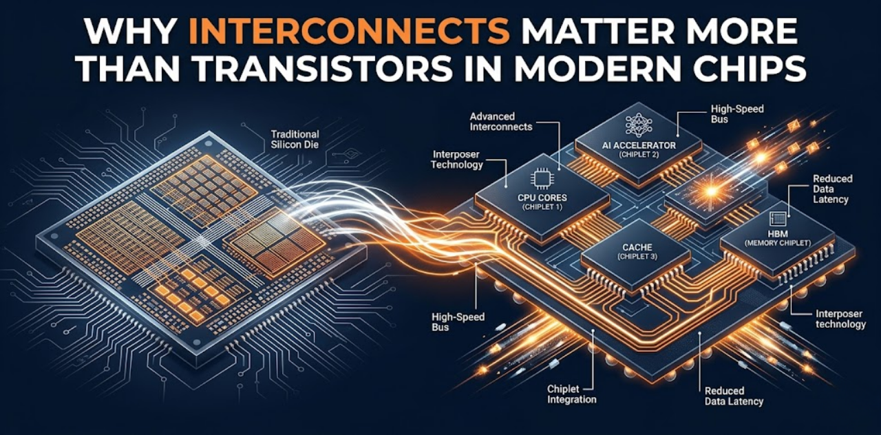
Advanced Packaging
Technologies such as:
- 2.5D Integration
- 3D Packaging
- Chiplet Architectures
reduce communication distances between components.
Backside Power Delivery
Separating power delivery from signal routing frees valuable routing resources and improves overall interconnect efficiency.
New Interconnect Materials
Researchers are exploring alternatives to copper, including:
- Ruthenium
- Cobalt
- Carbon nanotubes
- Graphene-based conductors
These materials may offer lower resistance at future nodes.
Silicon Photonics
Optical communication can transfer data using light rather than electrical signals.
Benefits include:
- Higher bandwidth
- Lower latency
- Reduced power consumption
Many experts view silicon photonics as a long-term solution to interconnect limitations.
The Future: Interconnect-Centric Chip Design
The semiconductor industry’s focus is gradually shifting from transistor scaling to communication optimization.
Future innovations will likely emphasize:
- Chiplet-based architectures
- Optical interconnects
- Monolithic 3D integration
- Advanced packaging technologies
- AI-optimized communication fabrics
- Near-memory and in-memory computing
Instead of asking how many transistors can fit on a chip, engineers are increasingly asking:
How efficiently can those transistors communicate?
This shift represents one of the most significant changes in semiconductor design philosophy over the last several decades.
Conclusion
Transistors remain the foundation of modern electronics, but their rapid scaling has exposed a new challenge: communication. As chips become increasingly complex, interconnects have emerged as the dominant factor influencing performance, power consumption, and scalability.
The future of semiconductor innovation will depend not only on building better transistors but also on developing faster, smarter, and more efficient ways to move data across chips. Technologies such as advanced packaging, chiplets, silicon photonics, and backside power delivery are all aimed at solving this growing challenge.
In the coming years, the winners of the semiconductor race may not be those with the smallest transistors but those with the smartest interconnect architectures.
Share your question in comments or talk to our mentor team for batch guidance.
Ask the Admin Team
Drop your basic question in comments: eligibility, prerequisites, tools, fee range, and placement support.
Our team reviews and responds regularly.
