For decades, processor performance improvements were driven by packing more transistors onto a single silicon die. However, as process nodes continue to shrink, designing large monolithic chips has become increasingly difficult, expensive, and risky.
Manufacturing challenges, rising wafer costs, lower yields, and growing design complexity are forcing the industry to rethink traditional chip design approaches.
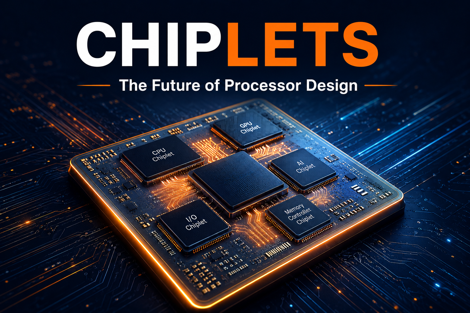
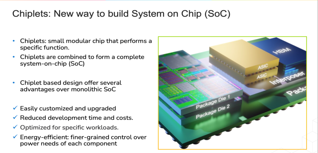
This has led to the rise of Chiplets a revolutionary architecture that breaks a large processor into smaller, specialized silicon dies connected within a single package. Chiplets are rapidly becoming the foundation of next-generation CPUs, GPUs, AI accelerators, and data center processors.
What Are Chiplets?
A chiplet is a smaller functional silicon block designed to perform a specific task within a larger processor system.
Instead of building one massive chip, manufacturers divide functionality into multiple chiplets such as:
- Compute Chiplets (CPU cores)
- Graphics Chiplets (GPU engines)
- AI Accelerator Chiplets
- Cache Chiplets
- Memory Controllers
- I/O Chiplets
These chiplets are integrated together using advanced packaging technologies to function as a single processor.
This modular approach allows designers to mix and match different technologies, process nodes, and functions while reducing manufacturing complexity.
Why Chiplets Are Transforming Processor Design
Improved Manufacturing Yield
Smaller dies have fewer manufacturing defects compared to large monolithic chips. Higher yield means more usable chips per wafer and significantly lower production costs.
Lower Development Costs
Designing multiple reusable chiplets is often more cost-effective than creating entirely new monolithic processors for every product generation.
Process Node Optimization
Not every component benefits equally from the latest manufacturing node.
For example:
- CPU cores may use advanced 2nm or 3nm technology.
- I/O controllers can remain on mature nodes.
- Analog circuits may stay on specialized processes.
Chiplets enable each function to be manufactured using the most suitable technology.
Faster Product Development
Reusable chiplet libraries allow semiconductor companies to develop new products faster while reducing engineering effort.
Greater Scalability
Manufacturers can scale performance by simply increasing the number of compute chiplets rather than redesigning an entire processor.
The Technologies Enabling Chiplets
Chiplet-based systems rely heavily on advanced packaging and high-speed interconnect technologies.
Advanced Packaging
Modern packaging techniques provide ultra-short, high-bandwidth connections between chiplets.
Examples include:
- 2.5D Packaging
- 3D Packaging
- Fan-Out Packaging
- Silicon Interposers
High-Speed Die-to-Die Communication
Chiplets must communicate with extremely low latency and high bandwidth.
Key interconnect technologies include:
- UCIe (Universal Chiplet Interconnect Express)
- Infinity Fabric
- EMIB
- CoWoS
- Foveros
These technologies allow multiple dies to behave like a single integrated processor.
Heterogeneous Integration
Different chiplets can be combined regardless of process node, vendor, or function, creating highly optimized computing platforms.
Applications of Chiplet-Based Architectures
Data Center Processors
Modern server CPUs require hundreds of cores and massive cache capacity. Chiplets enable scalable architectures that would be difficult to achieve with a single die.
Artificial Intelligence Accelerators
AI workloads demand enormous computational power and memory bandwidth. Chiplets allow AI processors to integrate compute, memory, and networking functions efficiently.
High-Performance Computing (HPC)
Supercomputers increasingly rely on chiplet architectures to achieve exascale performance while managing power and manufacturing costs.
Consumer Processors
Desktop and laptop CPUs are already benefiting from chiplet designs, enabling better performance, flexibility, and cost efficiency.
Automotive and Edge Computing
Future autonomous systems and edge AI platforms are expected to leverage chiplet architectures for customized processing solutions.
Conclusion
The future of processor design is no longer centered on building larger monolithic chips. Instead, it is focused on intelligently integrating multiple specialized chiplets into a unified system.
By delivering higher scalability, improved yields, lower costs, faster innovation cycles, and greater design flexibility, chiplets are redefining how modern processors are built. As AI, cloud computing, and high-performance computing continue to grow, chiplet architectures will play a critical role in shaping the next generation of semiconductor technology.
Share your question in comments or talk to our mentor team for batch guidance.
Ask the Admin Team
Drop your basic question in comments: eligibility, prerequisites, tools, fee range, and placement support.
Our team reviews and responds regularly.
