

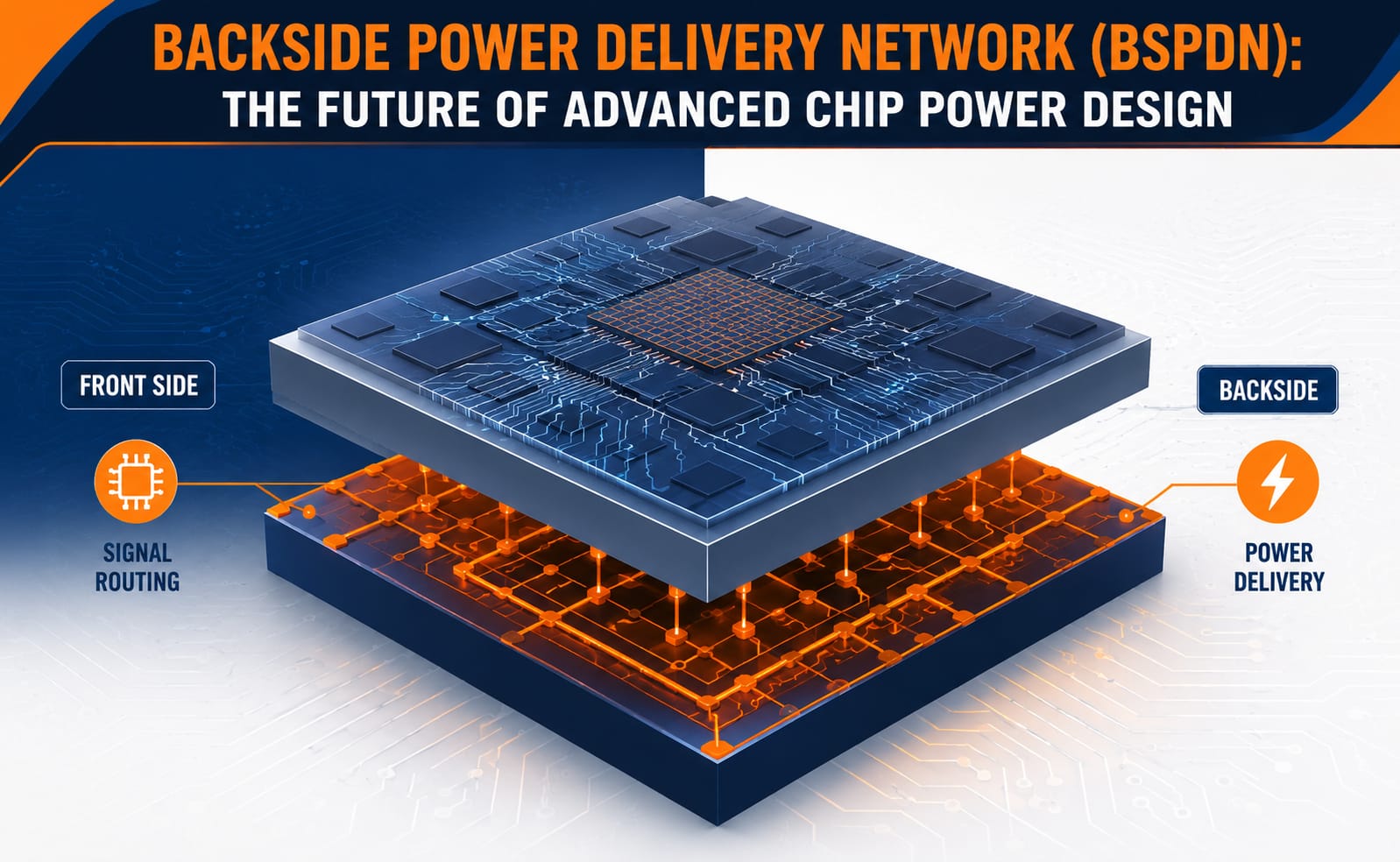
Backside Power Delivery Network (BSPDN) is an advanced semiconductor technology that moves the chip’s power delivery system from the traditional front side to the backside of the silicon wafer.
As transistor sizes continue shrinking, delivering stable power efficiently has become a major challenge. BSPDN helps improve power distribution while creating more space for signal routing.
Why Do Chips Need BSPDN?
In conventional chip designs, power and signal connections share the same front-side metal layers.
This creates challenges such as:
- Routing congestion
- Increased resistance
- Higher power loss
- Signal interference
- Limited space for scaling
BSPDN separates power delivery from signal routing, improving overall chip efficiency.
How BSPDN Works?
Traditional approach:
- Power lines → Front side of chip
- Signal lines → Same routing area
BSPDN approach:
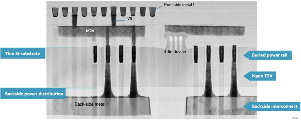
- Power network → Backside of silicon
- Signal routing → Front side
The backside contains dedicated power rails that supply energy directly to transistors through advanced connections.
Benefits of BSPDN in Advanced Nodes
BSPDN enables:
- Better Power Efficiency
Reduces voltage drop and power losses. - Improved Performance
Shorter power paths help deliver power faster. - Lower Routing Congestion
More front-side space becomes available for signal connections. - Higher Chip Density
Supports advanced nodes like 2nm and beyond.
BSPDN and Future Semiconductor Technologies
BSPDN plays an important role in next-generation chips used for:
- AI processors
- High-performance computing
- Data center chips
- Mobile processors
- Advanced chiplets
It works together with technologies like:
- 3D ICs
- Advanced packaging
- Gate-all-around transistors
- Hybrid bonding
Future of BSPDN
As semiconductor scaling moves beyond traditional limits, improving power delivery becomes as important as shrinking transistors.
Backside Power Delivery Network (BSPDN) represents a major shift in chip architecture, enabling faster, cooler, and more power-efficient semiconductor devices for future computing.
Share your question in comments or talk to our mentor team for batch guidance.
Ask the Admin Team
Drop your basic question in comments: eligibility, prerequisites, tools, fee range, and placement support.
Our team reviews and responds regularly.