

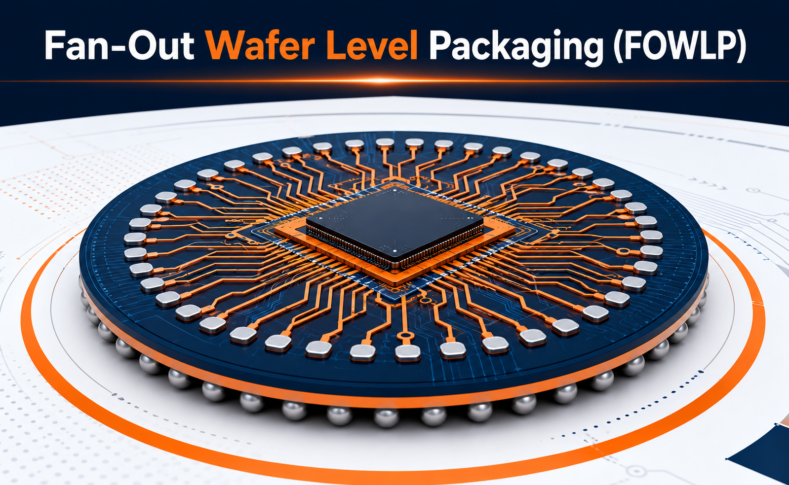
Fan-Out Wafer Level Packaging (FOWLP) is an advanced semiconductor packaging technology that improves chip performance by creating more space for electrical connections outside the silicon die.
Unlike traditional packaging methods, FOWLP allows redistribution layers (RDLs) to extend beyond the chip area, enabling higher I/O density, smaller package size, and better performance.
It is widely used in modern applications such as AI devices, smartphones, automotive electronics, and high-performance computing systems.
Why Is FOWLP Important?
Traditional packages face limitations in size, heat, and connectivity. FOWLP solves these challenges by providing:
- Smaller form factor – Enables thinner and lighter devices.
- Higher I/O capability – Supports more connections in limited space.
- Lower power consumption – Reduces signal loss and energy usage.
- Improved thermal performance – Helps manage heat efficiently.
FOWLP supports the continuous scaling demands of advanced semiconductor systems.
FOWLP in Modern Semiconductor Applications
FOWLP is becoming a key technology for next-generation electronics.
Major applications include:
- Mobile Processors – Compact and efficient chip designs.
- 5G Devices – High-frequency communication modules.
- AI & Data Centers – Advanced chip integration and performance improvement.
- Automotive Chips – Reliable and efficient electronics for smart vehicles.
It also supports heterogeneous integration by combining different chip technologies in one package.
Challenges and Future Development
Although FOWLP offers many benefits, some challenges remain:
- Complex manufacturing processes
- Warpage control issues
- Higher production complexity
- Thermal management challenges
Future improvements focus on larger wafer processing, advanced RDL technology, and integration with chiplet architectures.
Conclusion
Fan-Out Wafer Level Packaging is transforming semiconductor packaging by enabling smaller, faster, and more powerful electronic systems.
As chip designs become more complex, FOWLP will play a major role in AI computing, advanced processors, and next-generation semiconductor technologies.
FOWLP is helping move the industry from chip scaling to advanced system-level integration.
Share your question in comments or talk to our mentor team for batch guidance.
Ask the Admin Team
Drop your basic question in comments: eligibility, prerequisites, tools, fee range, and placement support.
Our team reviews and responds regularly.