As semiconductor technology has progressed toward increasingly smaller process nodes, traditional planar transistors have encountered significant challenges in maintaining performance, reducing power consumption, and controlling leakage current. The need for more efficient transistor architectures led to one of the most important innovations in modern chip manufacturing FinFET (Fin Field-Effect Transistor) technology.
FinFET technology revolutionized semiconductor fabrication by introducing a three-dimensional transistor structure that provides superior electrical control, enabling higher performance and improved energy efficiency. Today, FinFET remains a cornerstone of advanced semiconductor manufacturing, powering everything from smartphones and laptops to AI processors and data center chips.
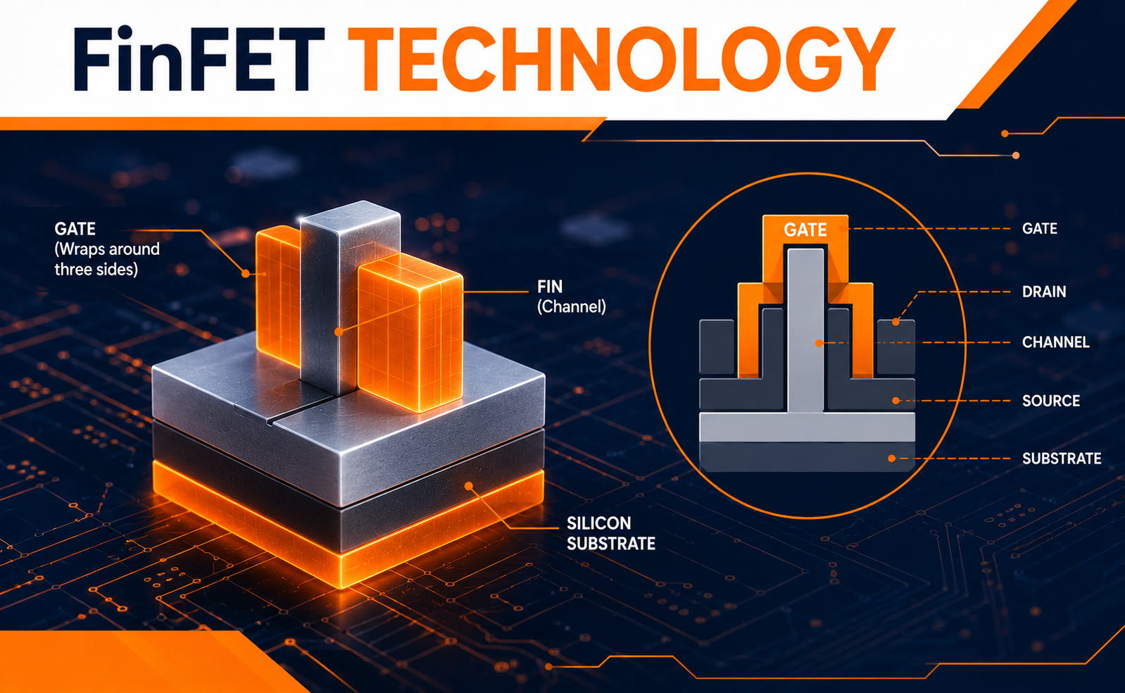
What is FinFET Technology?
FinFET (Fin Field-Effect Transistor) is a three-dimensional transistor architecture in which the conducting channel is formed as a thin vertical “fin” extending above the silicon substrate. Unlike traditional planar transistors, where the gate controls the channel from only one side, a FinFET gate wraps around the fin on three sides.
This innovative structure offers significantly better electrostatic control over current flow, helping reduce leakage while improving switching performance.
Key characteristics of FinFET technology include:
- Three-dimensional transistor structure
- Gate control on three sides of the channel
- Reduced leakage current
- Higher switching speed
- Lower operating voltage
- Improved power efficiency
- Better scalability for advanced process nodes
Why FinFET Replaced Planar Transistors
As transistor dimensions continued shrinking below 22nm, conventional planar MOSFETs faced several limitations:
- Increased leakage current
- Short-channel effects
- Higher power consumption
- Reduced gate control
- Performance degradation at smaller geometries
FinFET technology addressed these issues by improving gate control over the channel, allowing transistors to operate efficiently at much smaller dimensions.
This transition enabled semiconductor manufacturers to continue scaling integrated circuits while maintaining performance and reliability.
How FinFET Technology Works
The defining feature of FinFET is its vertical fin-shaped channel.
The operating principle involves:
- A thin silicon fin forms the transistor channel.
- The gate electrode wraps around three sides of the fin.
- Applying voltage to the gate controls electron flow through the channel.
- The improved gate coverage minimizes leakage current and enhances switching characteristics.
Multiple fins can also be combined within a single transistor to increase drive current and optimize performance for different applications.
Applications of FinFET Technology
FinFET technology has become the standard transistor architecture for advanced semiconductor devices.
Major applications include:
High-Performance Processors
Modern CPUs and GPUs use FinFET technology to deliver higher processing speeds while reducing power consumption.
Artificial Intelligence Accelerators
AI chips rely on FinFET transistors for improved computational efficiency and higher transistor density.
Mobile Processors
Smartphones and tablets benefit from FinFET’s low-power operation, extending battery life without sacrificing performance.
Data Centers and Cloud Computing
Server processors utilize FinFET technology to improve energy efficiency and computational performance for large-scale workloads.
Automotive Electronics
Advanced driver-assistance systems (ADAS), infotainment platforms, and autonomous driving processors leverage FinFET for reliable, high-performance operation.
Advantages
- Higher transistor density
- Lower leakage current
- Reduced power consumption
- Faster switching speeds
- Improved thermal efficiency
- Better short-channel control
- Enhanced overall chip performance
The Future of FinFET Technology
Although newer transistor architectures such as Gate-All-Around (GAA) and RibbonFET are emerging, FinFET remains a critical technology for many advanced semiconductor products.
Future developments include:
- Continued optimization for mature and advanced process nodes
- Integration with chiplet-based architectures
- Enhanced support for AI and high-performance computing
- Improved manufacturing efficiency through advanced lithography and process control
- Coexistence with GAA technologies during the industry’s transition to future nodes
FinFET will continue to serve as a foundational transistor technology while enabling a smooth evolution toward the next generation of semiconductor devices.
Conclusion
FinFET technology transformed the semiconductor industry by overcoming the limitations of planar transistors and enabling continued transistor scaling. Its three-dimensional architecture delivers superior performance, lower power consumption, and improved reliability, making it the backbone of modern integrated circuits..
Share your question in comments or talk to our mentor team for batch guidance.
Ask the Admin Team
Drop your basic question in comments: eligibility, prerequisites, tools, fee range, and placement support.
Our team reviews and responds regularly.
