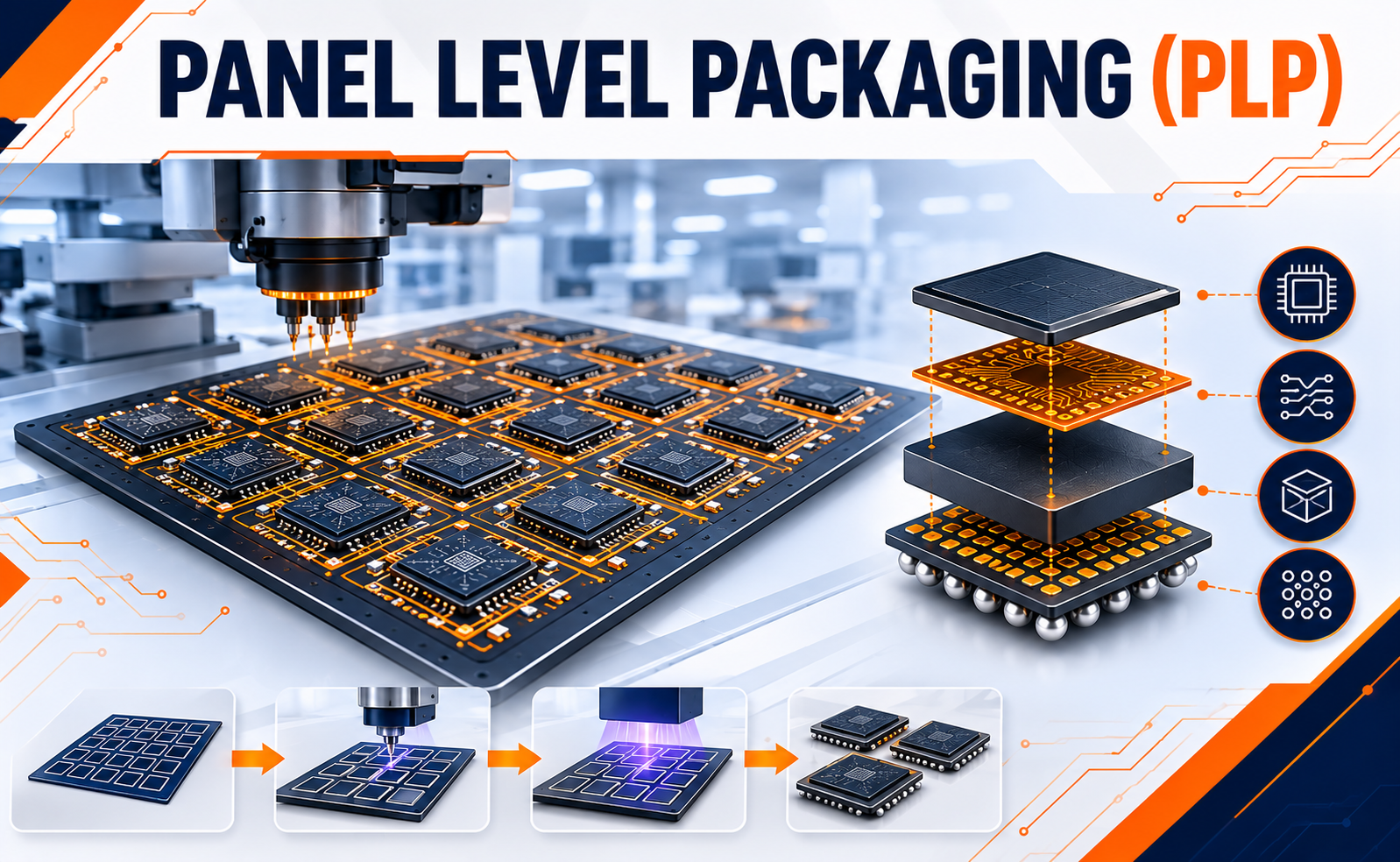
As semiconductor devices become more powerful and compact, the demand for cost-effective, high-performance packaging solutions continues to grow. Traditional wafer-based packaging technologies have served the industry for decades, but the increasing complexity of AI processors, automotive electronics, IoT devices, and high-performance computing systems has accelerated the need for more scalable manufacturing methods.
Panel Level Packaging (PLP) has emerged as a next-generation advanced packaging technology that replaces circular silicon wafers with large rectangular panels during the packaging process. This innovative approach increases manufacturing efficiency, reduces production costs, and enables higher packaging density, making PLP one of the most promising technologies for future semiconductor manufacturing.
What is Panel Level Packaging (PLP)?
Panel Level Packaging (PLP) is an advanced semiconductor packaging technology in which multiple semiconductor packages are fabricated simultaneously on large rectangular panels instead of conventional round wafers.
By utilizing larger substrates, manufacturers can process significantly more devices in a single production cycle, improving productivity while lowering manufacturing costs.
A typical PLP process supports:
- Multiple semiconductor dies
- Redistribution Layers (RDLs)
- Embedded passive components
- Fan-Out packaging structures
- Chiplet integration
- High-density interconnects
Why Panel Level Packaging is Transforming the Industry
Conventional wafer-level packaging is limited by the size of circular wafers, restricting the number of packages produced per manufacturing cycle.
Panel Level Packaging overcomes these limitations by offering:
- Larger manufacturing area
- Higher production throughput
- Lower cost per package
- Better material utilization
- Increased manufacturing efficiency
- Improved scalability for high-volume production
Applications of Panel Level Packaging
PLP is becoming increasingly important across a wide range of semiconductor applications.
Artificial Intelligence (AI)
Supports high-density AI accelerators requiring advanced interconnects and efficient power delivery.
High-Performance Computing (HPC)
Enables large processor packages with improved bandwidth and reduced manufacturing costs.
Automotive Electronics
Provides reliable packaging solutions for ADAS, autonomous driving systems, radar modules, and vehicle control units.
Consumer Electronics
Used in smartphones, tablets, wearable devices, and compact electronic products requiring miniaturized packaging.
Internet of Things (IoT)
Facilitates high-volume production of compact, energy-efficient semiconductor modules for connected devices.
The Future of Panel Level Packaging
Panel Level Packaging is expected to become a key enabler of future semiconductor manufacturing as demand grows for larger, more powerful, and cost-efficient electronic systems.
Emerging trends include:
- Ultra-high-density redistribution layers
- Chiplet-based heterogeneous integration
- AI accelerator packaging
- Integration with glass substrates
- Advanced Fan-Out Panel Level Packaging (FOPLP)
- Support for 2.5D and 3D package architectures
- AI-driven manufacturing optimization
Conclusion
Panel Level Packaging (PLP) represents a significant advancement in semiconductor packaging by enabling large-area, high-volume manufacturing with improved efficiency and reduced costs. By replacing traditional wafer-based processing with rectangular panel substrates, PLP delivers greater scalability, higher package density, and enhanced manufacturing productivity.
Share your question in comments or talk to our mentor team for batch guidance.
Ask the Admin Team
Drop your basic question in comments: eligibility, prerequisites, tools, fee range, and placement support.
Our team reviews and responds regularly.