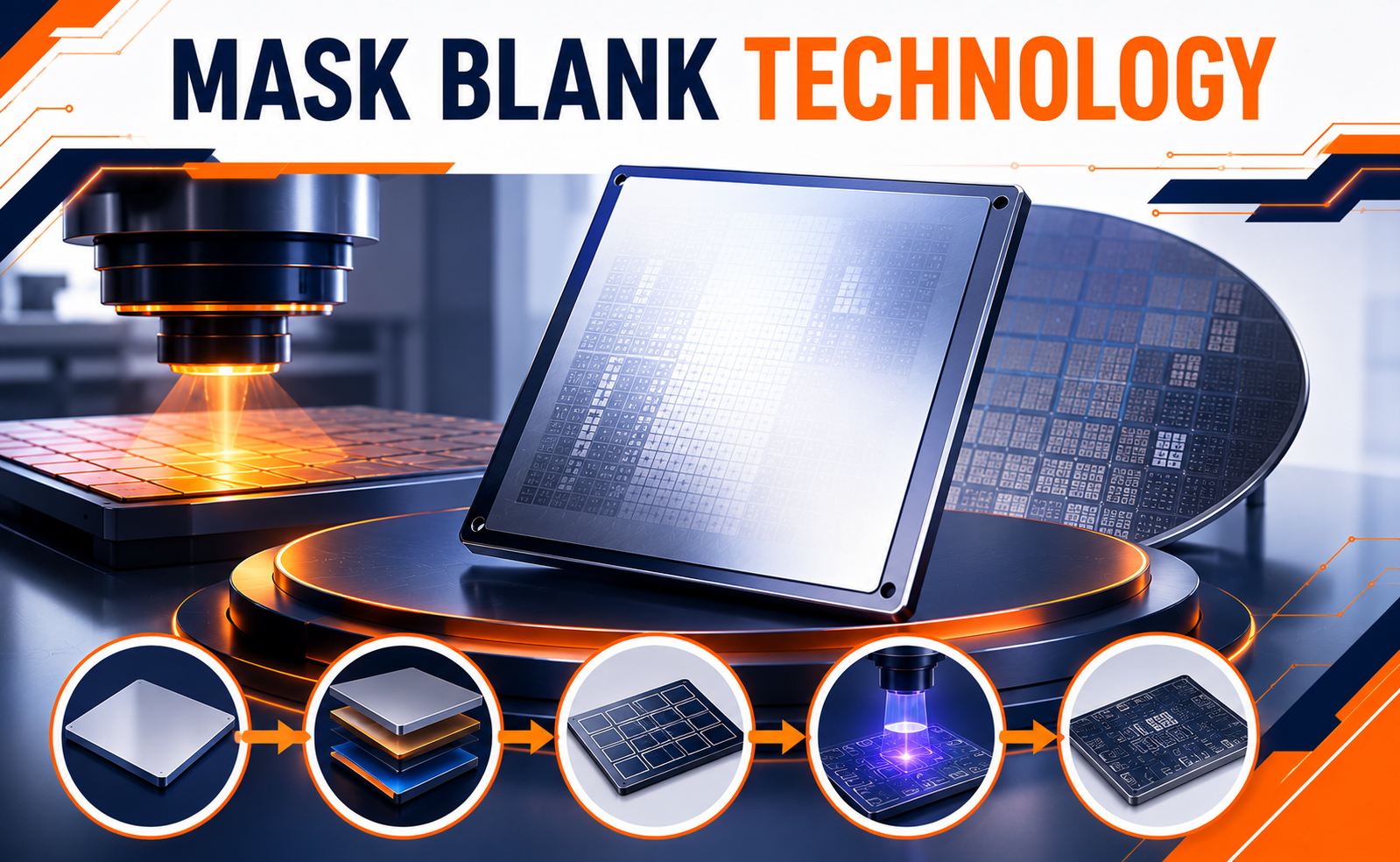
Modern semiconductor chips contain billions of microscopic transistors and interconnects that must be patterned with nanometer-level precision. Achieving this level of accuracy requires advanced photolithography, where intricate circuit patterns are transferred onto silicon wafers. At the heart of this process lies Mask Blank Technology, a critical component that serves as the foundation for creating high-precision photomasks.
A mask blank is the pristine substrate on which circuit patterns are written before being used during lithography. As semiconductor manufacturing advances toward 3nm, 2nm, and beyond, mask blank technology has become increasingly sophisticated, enabling the production of defect-free masks essential for advanced logic, memory, and AI chips.
What is Mask Blank Technology?
Mask Blank Technology refers to the fabrication of ultra-high-quality blank photomask substrates that are later patterned to create semiconductor masks used during photolithography.
A mask blank consists of several precisely engineered layers designed to ensure exceptional optical performance and defect control.
Typical components include:
- Ultra-flat quartz substrate
- Reflective multilayer coating (for EUV masks)
- Absorber layer
- Protective capping layer
- Anti-contamination coating
- Defect-free surface preparation
Why Mask Blank Technology is Critical
As semiconductor feature sizes continue shrinking, even the smallest defect on a photomask can be replicated across thousands of chips, resulting in yield loss and increased manufacturing costs.
Mask Blank Technology provides several essential benefits:
- Ultra-low defect density
- Superior optical performance
- High dimensional accuracy
- Excellent surface flatness
- Improved pattern fidelity
- Enhanced lithography precision
- Higher semiconductor manufacturing yield
Applications of Mask Blank Technology
Mask Blank Technology is essential across nearly every area of semiconductor manufacturing.
Advanced Logic Devices
Used to manufacture photomasks for processors, GPUs, AI accelerators, and networking chips.
Memory Manufacturing
Supports the fabrication of DRAM, SRAM, and 3D NAND Flash memory devices with extremely fine feature sizes.
EUV Lithography
Provides the highly reflective mask blanks required for Extreme Ultraviolet (EUV) lithography at advanced technology nodes.
Automotive Electronics
Enables the production of highly reliable semiconductor devices for ADAS, electric vehicles, and autonomous driving systems.
High-Performance Computing
Supports cutting-edge processors used in supercomputers, cloud infrastructure, and AI data centers.
The Future of Mask Blank Technology
As semiconductor manufacturing moves toward sub-2nm process nodes and High-NA EUV lithography, mask blank technology will continue evolving to support increasingly demanding fabrication requirements.
Future developments include:
- High-NA EUV-compatible mask blanks
- Advanced multilayer mirror technologies
- Improved defect-free substrate manufacturing
- AI-powered defect inspection systems
- Higher reflectivity coatings
- Enhanced contamination control
- Sustainable manufacturing processes with improved material efficiency
Conclusion
Mask Blank Technology is a foundational element of semiconductor manufacturing, providing the defect-free substrates required to produce precision photomasks. Every advanced chip, from AI processors and smartphones to automotive electronics and high-performance computing systems, depends on the quality and accuracy of these mask blanks.
Share your question in comments or talk to our mentor team for batch guidance.
Ask the Admin Team
Drop your basic question in comments: eligibility, prerequisites, tools, fee range, and placement support.
Our team reviews and responds regularly.