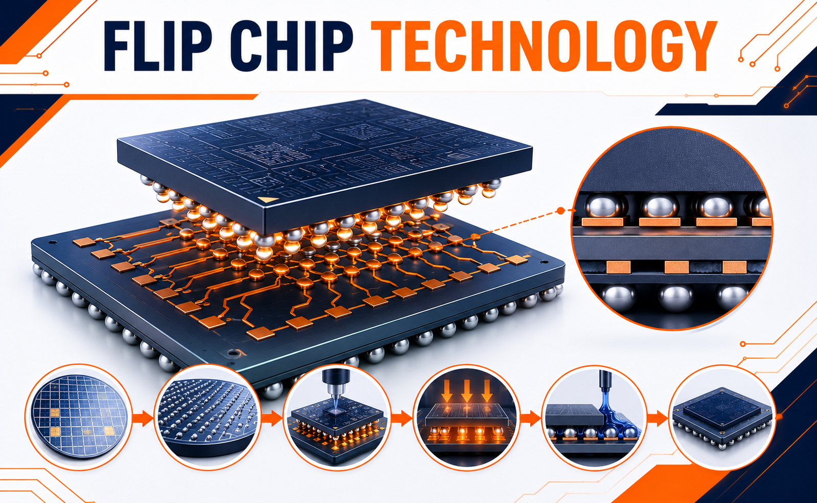
As semiconductor devices continue to demand higher performance, greater functionality, and smaller form factors, traditional wire bonding technologies face limitations in electrical performance, power delivery, and package density. To overcome these challenges, the semiconductor industry has widely adopted Flip Chip Technology, one of the most advanced interconnection methods used in modern integrated circuit packaging.
Unlike conventional wire-bonded packages, Flip Chip mounts the semiconductor die face-down onto the package substrate using microscopic solder bumps. This direct electrical connection provides shorter signal paths, improved thermal performance, and higher input/output (I/O) density, making Flip Chip a preferred packaging solution for high-performance processors, AI accelerators, GPUs, networking devices, and advanced semiconductor applications.
What is Flip Chip Technology?
Flip Chip is an advanced semiconductor packaging technology in which the integrated circuit (IC) die is flipped upside down and directly connected to the package substrate using an array of solder bumps instead of traditional wire bonds.
The primary components of a Flip Chip package include:
- Silicon die
- Solder bumps (micro-bumps or copper pillar bumps)
- Under Bump Metallization (UBM)
- Package substrate
- Underfill material
- Heat spreader or heat sink (for high-power devices)
Why Flip Chip is Important in Semiconductor Manufacturing
Flip Chip technology offers significant advantages over conventional wire bonding, making it essential for today’s advanced semiconductor devices.
Key benefits include:
- Higher I/O density
- Shorter electrical signal paths
- Lower parasitic resistance and inductance
- Improved signal integrity
- Better power distribution
- Enhanced thermal dissipation
- Smaller package footprint
- Support for high-speed and high-frequency applications
Applications of Flip Chip Technology
Flip Chip is widely used across a broad range of semiconductor products.
Artificial Intelligence (AI) Processors
Supports high-performance AI accelerators with superior power delivery and thermal management.
Central Processing Units (CPUs)
Used in modern desktop, server, and mobile processors requiring high-speed communication and dense interconnections.
Graphics Processing Units (GPUs)
Enables efficient heat dissipation and high-bandwidth operation for graphics and AI workloads.
High-Bandwidth Memory (HBM)
Provides reliable interconnections between memory stacks and logic dies in advanced computing systems.
Networking and Telecommunications
Used in high-speed switches, routers, ASICs, and communication processors for data centers and 5G infrastructure.
Automotive Electronics
Supports advanced driver-assistance systems (ADAS), autonomous vehicles, radar modules, and electric vehicle control systems.
The Future of Flip Chip Technology
As semiconductor devices continue to evolve, Flip Chip technology will remain a key enabler of next-generation packaging solutions.
Future developments include:
- Hybrid bonding integration
- Chiplet-based heterogeneous packaging
- Ultra-fine micro-bump technologies
- 2.5D and 3D IC integration
- Glass substrate compatibility
- AI-driven packaging process optimization
- Advanced thermal management solutions
- High-density fan-out packaging integration
Conclusion
Flip Chip Technology has transformed semiconductor packaging by replacing traditional wire bonds with direct solder bump interconnections. This innovative approach delivers superior electrical performance, higher interconnect density, improved thermal management, and enhanced reliability, making it indispensable for modern high-performance semiconductor devices.
Share your question in comments or talk to our mentor team for batch guidance.
Ask the Admin Team
Drop your basic question in comments: eligibility, prerequisites, tools, fee range, and placement support.
Our team reviews and responds regularly.