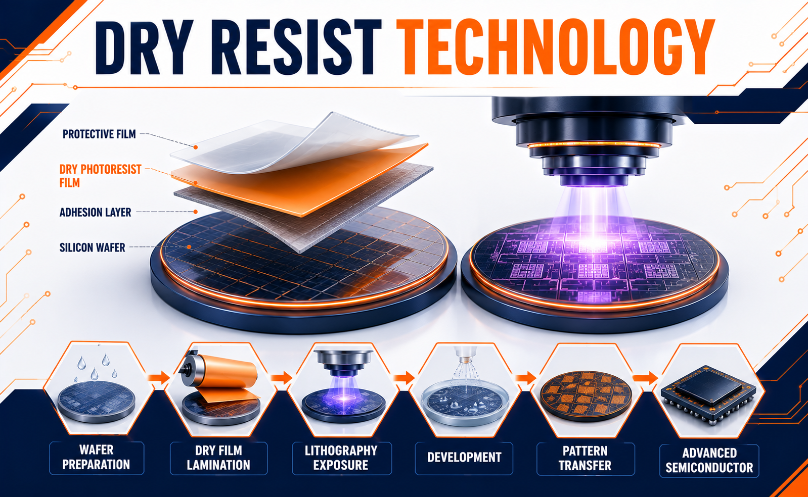
As semiconductor manufacturing moves toward advanced process nodes below 5nm and prepares for the next generation of High-NA EUV lithography, traditional photolithography materials face increasing challenges in resolution, process uniformity, and environmental sustainability. To meet these demands, the industry is adopting innovative patterning materials that offer greater precision and improved manufacturing efficiency.
Dry Resist Technology is one of the newest advancements in semiconductor lithography. Unlike conventional liquid photoresists, dry resist materials are supplied as thin films and laminated onto the wafer surface. This approach improves film uniformity, minimizes defects, reduces chemical waste, and enables the fabrication of extremely fine semiconductor features required for AI processors, advanced memory, and high-performance computing devices.
What is Dry Resist Technology?
Dry Resist Technology is an advanced lithography process that uses a pre-formed dry resist film instead of a liquid photoresist to create circuit patterns on semiconductor wafers.
The dry resist is laminated onto the wafer surface before exposure and development, providing highly uniform coverage and improved pattern fidelity.
Why Dry Resist Technology is Important
As semiconductor feature sizes continue shrinking, maintaining precise resist thickness and uniformity becomes increasingly difficult using conventional liquid coatings.
Dry Resist Technology offers several important advantages:
- Superior film thickness uniformity
- Reduced coating defects
- Higher pattern resolution
- Lower chemical consumption
- Improved process repeatability
- Better compatibility with advanced lithography
- Enhanced manufacturing sustainability
Applications of Dry Resist Technology
Dry Resist Technology is becoming increasingly important in advanced semiconductor manufacturing.
EUV Lithography
Supports extremely fine patterning required for advanced logic devices and future High-NA EUV systems.
Advanced Logic Processors
Enables fabrication of high-density CPUs, GPUs, and AI accelerators with improved pattern accuracy.
Memory Devices
Used in the production of DRAM and 3D NAND Flash memory requiring precise nanoscale features.
Advanced Packaging
Supports Redistribution Layer (RDL) formation and fine-line interconnects for Fan-Out, chiplet, and 3D packaging technologies.
Research and Development
Widely adopted in semiconductor process development for evaluating next-generation lithography materials and manufacturing techniques.
The Future of Dry Resist Technology
As semiconductor manufacturing advances toward sub-2nm technology nodes, Dry Resist Technology is expected to become an increasingly important component of future lithography processes.
Emerging developments include:
- High-NA EUV-compatible dry resists
- Ultra-high-resolution resist materials
- AI-assisted lithography process optimization
- Environmentally sustainable resist formulations
- Improved sensitivity for next-generation exposure systems
- Advanced materials for heterogeneous integration and chiplet packaging
- Enhanced defect control through precision film engineering
Conclusion
Dry Resist Technology represents a significant advancement in semiconductor patterning by replacing traditional liquid photoresists with highly uniform laminated resist films. Its ability to improve resolution, reduce defects, enhance process consistency, and support advanced EUV lithography makes it a promising solution for future semiconductor manufacturing.
Share your question in comments or talk to our mentor team for batch guidance.
Ask the Admin Team
Drop your basic question in comments: eligibility, prerequisites, tools, fee range, and placement support.
Our team reviews and responds regularly.