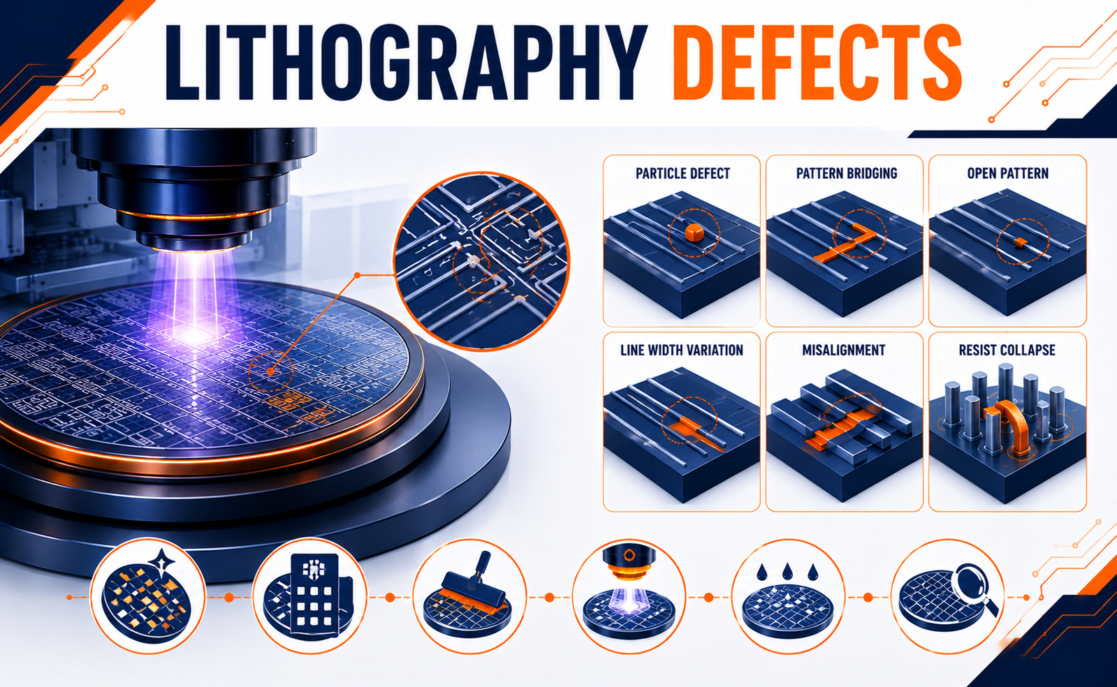
Photolithography is one of the most important processes in semiconductor manufacturing, responsible for transferring intricate circuit patterns onto silicon wafers with nanometer-level precision. As technology nodes continue shrinking to 5nm, 3nm, 2nm, and beyond, even the smallest lithography defect can significantly impact device performance, manufacturing yield, and production cost.
Lithography Defects are unintended imperfections that occur during the pattern transfer process due to issues in photomasks, photoresists, exposure systems, process conditions, or contamination. Detecting and minimizing these defects is essential for manufacturing advanced processors, memory devices, AI accelerators, automotive chips, and high-performance computing systems.
What are Lithography Defects?
Lithography Defects are unwanted pattern abnormalities that occur during the photolithography process, resulting in deviations from the intended circuit design on the semiconductor wafer.
These defects may originate from multiple sources, including:
- Photomask imperfections
- Photoresist coating issues
- Exposure system inaccuracies
- Focus and alignment errors
- Particle contamination
- Development process variations
- Optical distortions
Common Types of Lithography Defects
Several types of lithography defects are commonly observed during semiconductor manufacturing.
Particle Defects
Dust particles or contaminants block or scatter exposure light, causing missing or distorted circuit features.
Pattern Bridging
Adjacent circuit lines unintentionally connect due to excessive photoresist or exposure variations, leading to electrical short circuits.
Open Patterns
Incomplete pattern formation causes breaks in conductive paths, resulting in open circuits.
Line Width Variations
Changes in critical dimension (CD) produce inconsistent transistor sizes and electrical performance.
Misalignment Defects
Improper overlay between successive lithography layers affects interconnect accuracy and device functionality.
Photoresist Collapse
High-aspect-ratio resist structures bend or collapse during development, distorting the intended pattern.
Causes of Lithography Defects
Lithography defects arise from a combination of equipment limitations, material properties, and process variations.
Common causes include:
Mask Defects
Imperfections in photomasks or EUV masks transfer directly to the wafer pattern.
Focus and Exposure Errors
Incorrect exposure dose or focus settings result in blurred or incomplete pattern transfer.
Photoresist Issues
Non-uniform resist thickness, poor adhesion, or improper development can generate pattern defects.
Process Contamination
Airborne particles, chemical residues, and equipment contamination introduce unwanted imperfections.
Equipment Variations
Optical aberrations, stage positioning errors, and scanner calibration inaccuracies contribute to defect formation.
Maintaining strict process control is essential for minimizing these sources of variation.
Detection and Prevention of Lithography Defects
Semiconductor manufacturers employ advanced metrology and inspection systems to detect and minimize lithography defects.
Detection Techniques
- Optical inspection systems
- Electron beam (E-beam) inspection
- Critical Dimension Scanning Electron Microscopy (CD-SEM)
- Overlay measurement systems
- Defect review microscopes
- Automated wafer inspection tools
- AI-based defect classification systems
Prevention Strategies
- Ultra-clean cleanroom environments
- High-quality photomasks
- Precise exposure and focus calibration
- Optimized photoresist processing
- Advanced process control (APC)
- Regular equipment maintenance
- Continuous defect monitoring using AI and machine learning
These methods help manufacturers achieve higher yields and consistent process quality.
The Future of Lithography Defect Management
As semiconductor fabrication advances toward sub-2nm technologies and High-NA EUV lithography, defect control will become even more critical.
Emerging innovations include:
- AI-driven real-time defect detection
- Machine learning-based process optimization
- High-NA EUV-compatible inspection systems
- Advanced computational lithography
- Improved photoresist materials
- Next-generation mask inspection technologies
- Predictive maintenance for lithography equipment
Conclusion
Lithography Defects are among the most critical challenges in semiconductor manufacturing, directly influencing chip performance, yield, and reliability. From particle contamination and mask imperfections to photoresist issues and alignment errors, every stage of the lithography process requires precise control to achieve defect-free pattern transfer.
Share your question in comments or talk to our mentor team for batch guidance.
Ask the Admin Team
Drop your basic question in comments: eligibility, prerequisites, tools, fee range, and placement support.
Our team reviews and responds regularly.