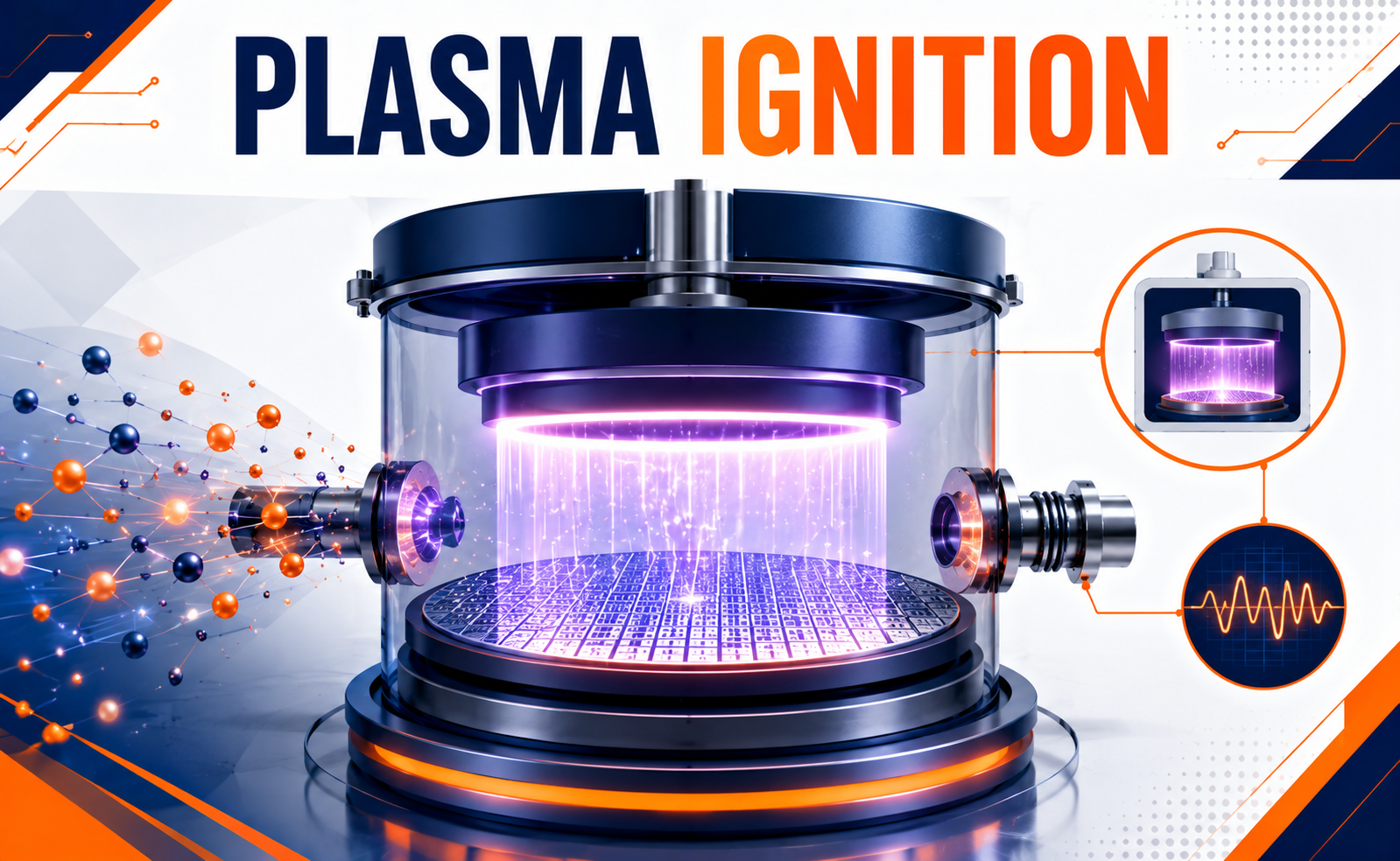
Modern semiconductor manufacturing relies heavily on plasma-based processes such as plasma etching, plasma cleaning, plasma-enhanced chemical vapor deposition (PECVD), and atomic layer etching (ALE). Before these processes can begin, a stable plasma must first be generated inside the process chamber. This critical initial stage is known as Plasma Ignition.
Plasma Ignition is the process of converting a neutral process gas into an ionized plasma using electrical energy. Once the plasma is ignited, it produces energetic ions, electrons, and reactive radicals that drive precise material removal, surface cleaning, or thin-film deposition. A stable and controlled plasma ignition process is essential for achieving high wafer yield, uniform processing, and reliable semiconductor device performance.
What is Plasma Ignition?
Plasma Ignition is the process of initiating a plasma discharge inside a semiconductor process chamber by applying electrical energy to a process gas under controlled pressure.
During ignition, gas molecules absorb energy and become ionized, creating a mixture of charged particles, free electrons, ions, and reactive radicals known as plasma.
Why Plasma Ignition is Important
A stable plasma is the foundation of many semiconductor fabrication processes. Improper plasma ignition can lead to poor process uniformity, defects, and reduced manufacturing yield.
Plasma Ignition provides several important advantages:
- Enables controlled plasma generation
- Ensures uniform wafer processing
- Improves etching precision
- Supports high-quality thin-film deposition
- Enhances process repeatability
- Reduces defect formation
- Improves equipment reliability
- Increases manufacturing efficiency
Applications of Plasma Ignition
Plasma Ignition is required in numerous semiconductor fabrication processes.
Plasma Etching
Initiates reactive plasma used to precisely remove silicon, dielectric, or metal layers.
Plasma Cleaning
Generates plasma for removing organic residues, particles, and contaminants from wafer surfaces.
PECVD (Plasma-Enhanced Chemical Vapor Deposition)
Creates plasma to enhance chemical reactions for depositing thin films at lower temperatures.
Atomic Layer Etching (ALE)
Supports controlled atomic-scale material removal through precisely generated plasma cycles.
Advanced Packaging
Used during surface activation and cleaning processes for wafer bonding, hybrid bonding, and advanced packaging technologies.
The Future of Plasma Ignition Technology
As semiconductor manufacturing advances toward sub-2nm process nodes and increasingly complex device architectures, plasma ignition technologies are also evolving.
Emerging developments include:
- AI-assisted plasma ignition control
- Real-time plasma monitoring systems
- Low-damage plasma generation
- High-uniformity plasma sources for 300 mm and future wafers
- Advanced RF matching technologies
- Energy-efficient plasma generation
- Improved plasma stability for High-NA EUV manufacturing
- Integration with next-generation atomic layer processing technologies
Conclusion
Plasma Ignition is the critical first step in every plasma-based semiconductor manufacturing process. By transforming process gases into a stable, highly reactive plasma, it enables precision etching, advanced cleaning, thin-film deposition, and atomic-scale material processing.
As semiconductor technologies continue to evolve, reliable and efficient plasma ignition will remain fundamental to producing faster, smaller, and more energy-efficient integrated circuits. Its role in supporting advanced fabrication processes makes it an indispensable technology in modern semiconductor manufacturing.
Share your question in comments or talk to our mentor team for batch guidance.
Ask the Admin Team
Drop your basic question in comments: eligibility, prerequisites, tools, fee range, and placement support.
Our team reviews and responds regularly.