

The semiconductor industry has continuously evolved transistor architectures to meet the growing demand for higher performance, lower power consumption, and increased transistor density. From planar CMOS to FinFETs and more recently Gate-All-Around (GAA) nanosheet transistors, each innovation has enabled chips to become faster and more energy-efficient. However, as technology advances toward the 1.4nm and Angstrom era, engineers require new transistor structures capable of overcoming the physical limitations of existing designs.
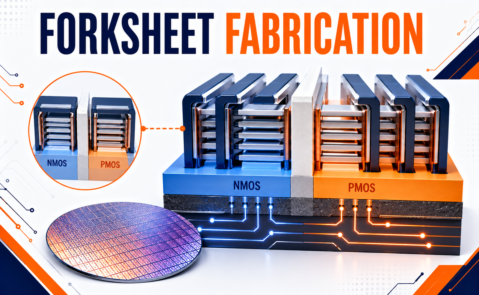
Forksheet Fabrication is an emerging transistor manufacturing technology designed to extend Moore’s Law beyond Gate-All-Around devices. By introducing a dielectric wall that separates the NMOS and PMOS transistors while allowing them to be placed much closer together, Forksheet architecture enables greater transistor density, improved electrostatic control, and enhanced performance. It is considered one of the most promising candidates for future logic technologies beyond today’s GAA transistors.
What is Forksheet Fabrication?
Forksheet Fabrication is an advanced semiconductor manufacturing process used to create Forksheet transistors, a next-generation evolution of Gate-All-Around (GAA) nanosheet transistors.
The defining feature of this architecture is a thin insulating dielectric wall positioned between adjacent NMOS and PMOS devices. This wall electrically isolates the transistors while allowing them to be placed much closer together than in conventional GAA designs.
Why Forksheet Technology is Important
As semiconductor nodes continue shrinking, reducing the distance between transistors becomes increasingly difficult due to electrical interference and manufacturing constraints.
Forksheet technology addresses these challenges by providing several key advantages:
- Higher transistor density
- Reduced standard cell area
- Improved electrostatic control
- Lower power consumption
- Higher switching performance
- Better routing efficiency
- Improved logic density
- Compatibility with future semiconductor nodes
Applications of Forksheet Technology
Although still under development, Forksheet transistors are expected to power a wide range of next-generation semiconductor products.
Artificial Intelligence (AI) Processors
Supports higher transistor density and improved energy efficiency for AI accelerators.
High-Performance Computing (HPC)
Enables faster processors with lower power consumption for servers and supercomputers.
Mobile Processors
Provides improved battery life and increased computing performance for smartphones and tablets.
Automotive Electronics
Supports high-performance processors used in autonomous driving systems and advanced vehicle electronics.
Data Centers and Cloud Computing
Improves processor efficiency while reducing energy consumption in large-scale computing environments.
The Future of Forksheet Fabrication
Forksheet technology is widely regarded as a bridge between today’s Gate-All-Around transistors and future transistor architectures such as Complementary FET (CFET).
Future developments include:
- High-NA EUV lithography for improved patterning
- AI-assisted process optimization
- Advanced dielectric materials
- Integration with Buried Power Rail (BPR) technology
- Enhanced nanosheet engineering
- Improved process uniformity
- Higher transistor density for Angstrom-era nodes
- Evolution toward vertically stacked CFET architectures
Conclusion
Forksheet Fabrication represents one of the most significant innovations in advanced transistor technology. By introducing a dielectric isolation wall within a Gate-All-Around architecture, it enables higher transistor density, improved electrical performance, and lower power consumption compared to existing transistor designs.
As the semiconductor industry moves beyond 2nm technology and into the Angstrom era, Forksheet transistors are expected to play a crucial role in enabling the next generation of AI processors, high-performance computing systems, mobile devices, and advanced electronics. Together with technologies such as Buried Power Rail and CFET, Forksheet Fabrication is helping shape the future of semiconductor manufacturing.
Share your question in comments or talk to our mentor team for batch guidance.
Ask the Admin Team
Drop your basic question in comments: eligibility, prerequisites, tools, fee range, and placement support.
Our team reviews and responds regularly.