

The performance and reliability of semiconductor devices begin with the quality of the silicon crystal used to manufacture wafers. As applications such as electric vehicles, renewable energy systems, high-voltage electronics, RF communication, and advanced sensors continue to grow, the demand for silicon with extremely low impurity levels has become more important than ever.
Float Zone (FZ) Technology is an advanced crystal growth process that produces ultra-high-purity single-crystal silicon without the use of a crucible. Unlike conventional crystal growth methods, Float Zone technology minimizes contamination from oxygen and other impurities, resulting in silicon with exceptional electrical characteristics. This makes FZ silicon the preferred choice for high-power, high-frequency, and radiation-resistant semiconductor devices.
What is Float Zone (FZ) Technology?
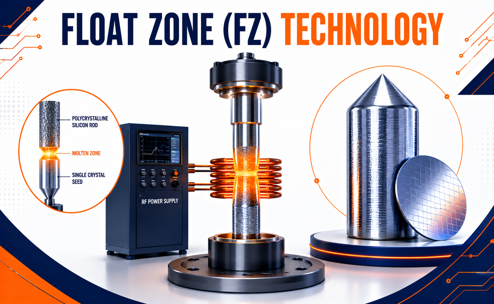
Float Zone (FZ) Technology is a semiconductor crystal growth process used to manufacture ultra-pure single-crystal silicon ingots.
Instead of melting silicon inside a crucible, a narrow molten zone is created using radio-frequency (RF) induction heating. This molten region slowly moves along a high-purity silicon rod, refining the crystal structure and removing impurities as it progresses.
Why Float Zone Technology is Important
Many advanced semiconductor applications require silicon with extremely low oxygen content and superior electrical performance.
Float Zone Technology offers several important advantages:
- Ultra-high silicon purity
- Extremely low oxygen contamination
- High electrical resistivity
- Excellent carrier lifetime
- Reduced crystal defects
- Superior thermal stability
- Enhanced device reliability
- Ideal for high-power semiconductor applications
Applications of Float Zone Silicon
Float Zone silicon is widely used in specialized semiconductor devices where high electrical performance is essential.
Power Semiconductors
Used in high-voltage MOSFETs, IGBTs, thyristors, and power diodes.
Electric Vehicles (EVs)
Supports efficient power conversion systems used in electric drivetrains and charging infrastructure.
RF and Microwave Devices
Provides superior substrates for high-frequency communication components.
Radiation-Hardened Electronics
Used in aerospace, defense, and satellite systems where resistance to radiation is critical.
Scientific and Industrial Equipment
Supports precision sensors, medical imaging systems, and advanced laboratory instrumentation.
The Future of Float Zone Technology
As advanced power electronics and high-performance semiconductor devices continue to evolve, Float Zone Technology is expected to remain an important manufacturing process.
Future developments include:
- AI-assisted crystal growth optimization
- Larger-diameter Float Zone silicon ingots
- Improved RF induction heating systems
- Enhanced crystal defect monitoring
- Higher manufacturing efficiency
- Advanced substrates for wide-bandgap semiconductor research
- Sustainable and energy-efficient crystal growth techniques
- Integration with next-generation power electronics and quantum technologies
Conclusion
Float Zone (FZ) Technology is one of the most advanced silicon crystal growth methods used in the semiconductor industry. By eliminating crucible-related contamination and producing ultra-high-purity single-crystal silicon, it delivers exceptional electrical performance, reliability, and material quality.
As industries increasingly rely on power electronics, electric vehicles, RF communication, aerospace systems, and advanced scientific equipment, Float Zone Technology will continue to play a vital role in supplying the premium silicon needed for next-generation semiconductor devices. Its unmatched purity and performance make it a cornerstone of high-end semiconductor manufacturing.
Share your question in comments or talk to our mentor team for batch guidance.
Ask the Admin Team
Drop your basic question in comments: eligibility, prerequisites, tools, fee range, and placement support.
Our team reviews and responds regularly.