

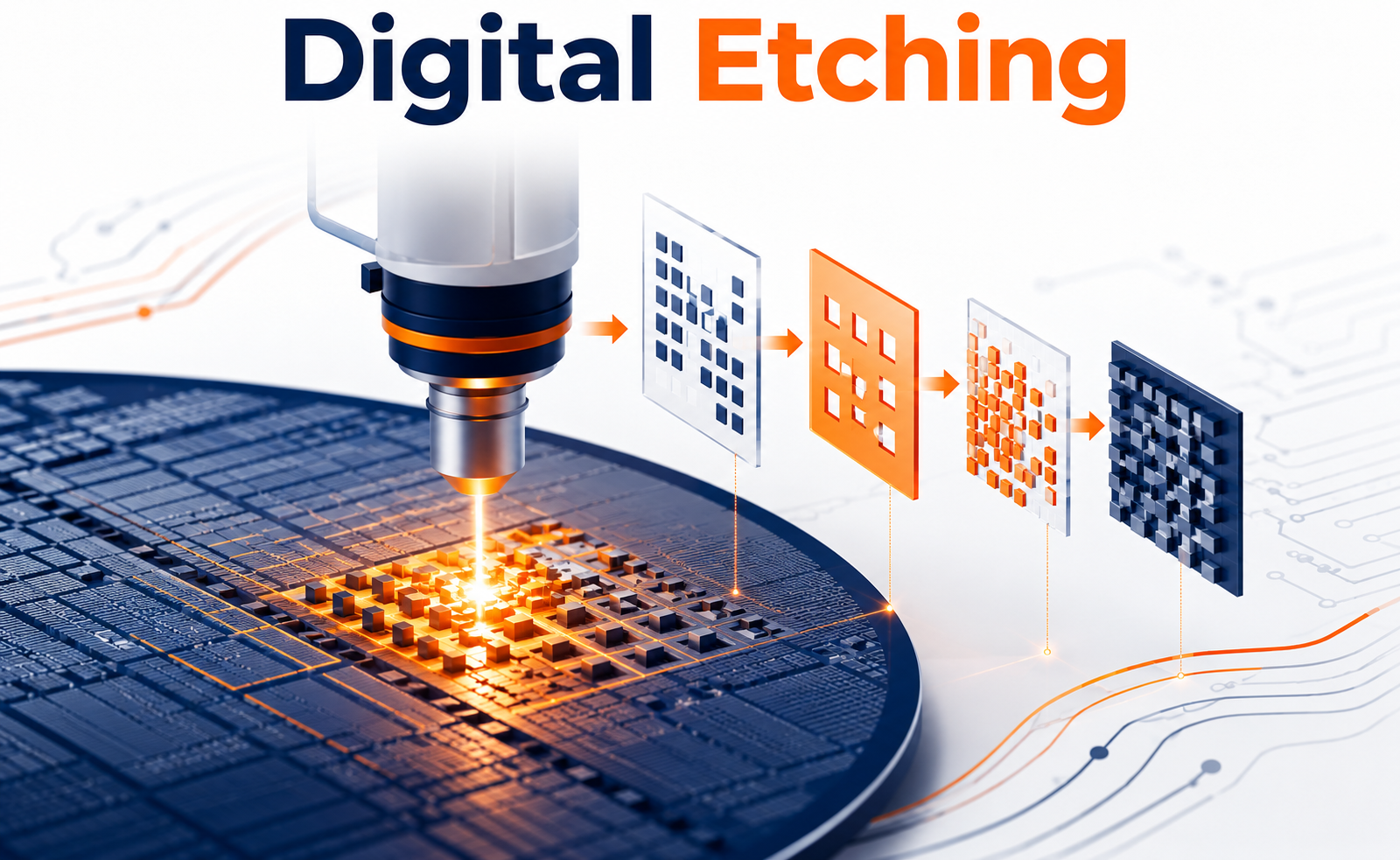
As semiconductor devices continue to shrink and become more complex, manufacturers need increasingly precise methods to shape and pattern materials at the nanoscale. Digital etching is an advanced etching approach that enables highly controlled material removal, often with excellent selectivity and near-atomic-scale precision.
Unlike conventional etching techniques that may continuously remove material, digital etching can use carefully controlled, sequential process steps to remove material in a highly predictable manner. This makes it particularly valuable for advanced semiconductor fabrication, where even a small amount of unwanted material removal can affect device performance.
How Digital Etching Works
Digital etching generally relies on a sequence of controlled surface reactions rather than a single continuous etching operation.
A typical process involves:
- Surface modification – A controlled chemical reaction modifies or prepares the target material’s surface.
- Selective removal – The modified surface layer is removed using a suitable process.
- Process repetition – The cycle is repeated to achieve the required etch depth.
Because the process can be divided into precisely controlled cycles, manufacturers can better manage etch depth, selectivity, surface damage, and profile control.
This cyclic approach is especially useful when fabricating extremely small semiconductor structures where conventional processes may provide insufficient control.
Digital Etching vs. Conventional Etching
Traditional etching processes are often designed for continuous material removal. While effective for many applications, they can become challenging as device dimensions approach the nanoscale.
Digital etching offers several potential advantages:
- High etch-depth control
- Improved material selectivity
- Reduced surface damage
- Better control of critical dimensions
- Potential for highly uniform processing
- Greater suitability for advanced device architectures
The key difference is process control. Digital etching focuses on precisely controlling how much material is removed during each cycle, helping engineers achieve more predictable nanoscale structures.
Applications in Semiconductor Manufacturing
Digital etching has growing relevance across advanced semiconductor fabrication. It can be particularly useful for structures where dimensional accuracy and material selectivity are critical.
Potential applications include:
Advanced Transistors
Modern transistor architectures such as FinFETs and gate-all-around (GAA) devices require precise formation and shaping of extremely small structures. Controlled etching can help maintain the intended device geometry.
3D Semiconductor Structures
As semiconductor manufacturing increasingly moves toward three-dimensional architectures, precise vertical and lateral material removal becomes essential.
High-Aspect-Ratio Structures
Digital etching can support the fabrication of structures where maintaining profile control and minimizing unwanted material loss are important.
Emerging Semiconductor Materials
New device concepts increasingly incorporate materials with different chemical and physical properties. Selective, controlled etching can help process these material stacks with greater precision.
Key Challenges and Process Considerations
Despite its advantages, digital etching presents several manufacturing challenges.
Process complexity is one of the major considerations. Each cycle must be carefully controlled to maintain consistent results across the wafer.
Other important factors include:
- Reaction uniformity across large wafer areas
- Surface chemistry control
- Etch selectivity between different materials
- Cycle-to-cycle consistency
- Throughput and manufacturing cost
- Integration with existing fabrication processes
As semiconductor geometries continue to shrink, engineers must balance precision, productivity, and scalability.
The Future of Digital Etching
The semiconductor industry is moving toward increasingly complex architectures, smaller dimensions, and new material combinations. These trends are creating a stronger demand for etching technologies capable of delivering precise and repeatable material removal.
Digital etching represents an important direction in this evolution. By combining controlled surface chemistry with carefully engineered removal cycles, it can provide manufacturers with greater control over nanoscale structures.
As advanced nodes, 3D devices, and emerging semiconductor technologies continue to develop, precise etching will remain a critical part of semiconductor manufacturing. Digital etching could play an increasingly important role in enabling the next generation of high-performance and highly integrated devices.
Share your question in comments or talk to our mentor team for batch guidance.
Ask the Admin Team
Drop your basic question in comments: eligibility, prerequisites, tools, fee range, and placement support.
Our team reviews and responds regularly.