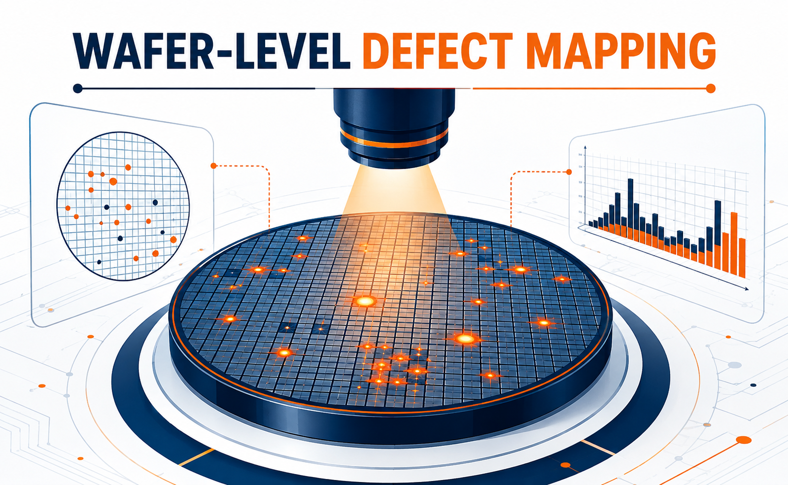
In semiconductor manufacturing, even a small defect can affect device performance, reliability, and overall yield. As wafer dimensions shrink and process complexity increases, identifying where defects occur, how frequently they appear, and what patterns they form becomes increasingly important.
Wafer-level defect mapping provides manufacturers with a visual and analytical method to understand defects across an entire wafer. By converting inspection data into spatial maps, engineers can identify systematic process issues, distinguish random defects from recurring patterns, and take corrective action before problems affect large production volumes.
What Is Wafer-Level Defect Mapping?
Wafer-level defect mapping is the process of detecting, locating, classifying, and visually representing defects across a semiconductor wafer.
During wafer inspection, different types of defects can be detected, including:
- Particle contamination
- Pattern defects
- Scratches
- Missing or abnormal structures
- Critical-dimension variations
- Open and short defects
- Process-induced abnormalities
Each detected defect is assigned a location on the wafer. These coordinates are then converted into a defect map, allowing engineers to see the spatial distribution of defects rather than analyzing individual defects independently.
This transforms large volumes of inspection data into a pattern that can be interpreted much more easily.
How Defect Mapping Works
Wafer-level defect mapping typically combines automated inspection systems, defect classification, coordinate data, and analytical software.
A simplified workflow is:
Wafer Inspection → Defect Detection → Coordinate Generation → Defect Classification → Wafer Map → Pattern Analysis → Root-Cause Investigation
Inspection tools scan the wafer surface and identify potential abnormalities. The system records the position and characteristics of each defect, while classification algorithms help categorize them.
The resulting map can show defects as points, symbols, or different categories across the wafer surface.
Engineers can then compare maps between wafers, lots, process steps, and manufacturing tools to identify recurring behavior.
Why Spatial Patterns Matter
One of the biggest advantages of defect mapping is that location itself can provide clues about the underlying process problem.
For example, different spatial distributions can indicate different sources:
- Random distribution: May indicate isolated contamination or random events.
- Edge concentration: Can point toward edge-related processing or handling issues.
- Center concentration: May indicate process uniformity or equipment-related effects.
- Ring-shaped patterns: Can be associated with process non-uniformity across the wafer.
- Repeating patterns: May indicate systematic process or lithography-related problems.
- Localized clusters: Can suggest contamination, equipment interaction, or localized process abnormalities.
The map does not automatically identify the root cause. Instead, it provides engineers with an important spatial signature that can be correlated with process and equipment data.
The Future of Wafer-Level Defect Mapping
As semiconductor technologies move toward increasingly small process nodes, advanced packaging, 3D structures, and more complex device architectures, defect analysis is becoming even more critical.
Future defect-mapping systems are expected to increasingly combine high-resolution inspection, automated classification, machine learning, process data, and predictive analytics.
The goal is not simply to create a map after a defect occurs. The larger objective is to recognize defect signatures early, identify their probable sources, and prevent recurring defects from propagating through production.
Conclusion
Wafer-level defect mapping is more than a visualization technique it is a powerful manufacturing analysis tool. By connecting defect location with process information, engineers can recognize spatial patterns, investigate root causes, improve process control, and protect semiconductor yield.
As wafer processes become more sophisticated, the ability to transform millions of inspection data points into actionable spatial intelligence will remain an essential part of modern semiconductor manufacturing.
Share your question in comments or talk to our mentor team for batch guidance.
Ask the Admin Team
Drop your basic question in comments: eligibility, prerequisites, tools, fee range, and placement support.
Our team reviews and responds regularly.