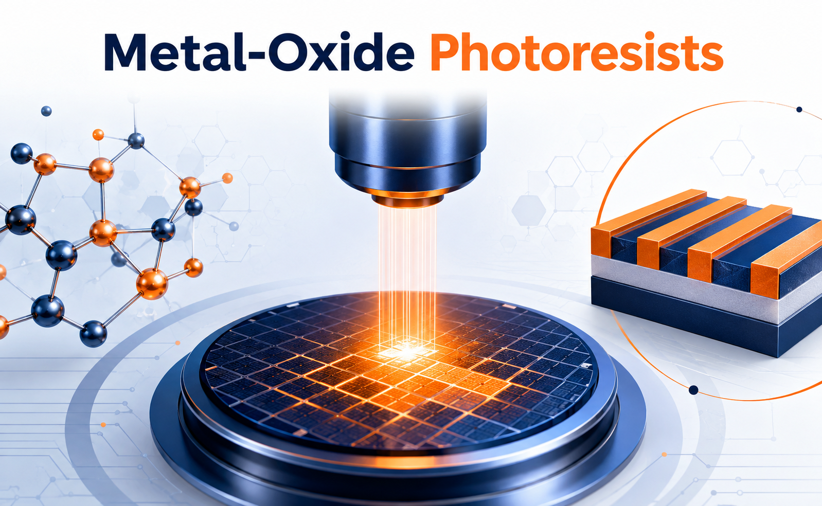
As semiconductor devices continue to scale toward smaller nodes, conventional organic photoresists face increasing challenges in achieving the resolution, sensitivity, and pattern fidelity required for advanced lithography. Metal-oxide photoresists (MORs) have emerged as a promising alternative, particularly for extreme ultraviolet (EUV) lithography.
By combining inorganic metal-oxide chemistry with photoresist functionality, MORs offer unique material properties that can support the fabrication of increasingly small and complex semiconductor patterns.
What Are Metal-Oxide Photoresists?
Metal-oxide photoresists are lithographic materials based on metal-oxide clusters or nanoparticles rather than traditional organic polymer chains. Common metal components include hafnium (Hf), zirconium (Zr), tin (Sn), and zinc (Zn).
When exposed to radiation such as EUV, the material undergoes chemical changes that modify its solubility in a developer. This allows selected regions to remain or be removed during development, producing the desired nanoscale pattern.
Their inorganic structure provides several advantages, including:
- High resistance to plasma-based etching
- Strong absorption of EUV radiation
- Potential for high-resolution patterning
- Improved mechanical and thermal stability
- Reduced pattern collapse at very small dimensions
Why Metal-Oxide Photoresists Matter for EUV Lithography
EUV lithography operates at a wavelength of approximately 13.5 nm, enabling semiconductor manufacturers to print extremely small features. However, creating high-quality patterns at these dimensions requires photoresists with carefully balanced properties.
MORs are attractive because their metal-containing components can interact efficiently with EUV radiation. This can generate the chemical reactions required for pattern formation while maintaining a relatively dense material structure.
For advanced lithography, the key challenge is achieving an appropriate balance between:
Resolution + Sensitivity + Line Edge Roughness
Improving one property can sometimes negatively affect another, making resist chemistry and process optimization critical.
Key Advantages and Challenges
Metal-oxide photoresists offer several potential benefits for advanced semiconductor manufacturing.
Key Advantages
- High resolution: Suitable for very small lithographic features.
- High EUV absorption: Metal elements can efficiently interact with EUV radiation.
- High etch resistance: Inorganic materials can withstand aggressive pattern-transfer processes.
- Thin-film capability: MORs can potentially support thin resist stacks.
- Improved pattern stability: Their material properties can help maintain nanoscale structures.
Key Challenges
Despite their potential, MORs still face important development challenges.
Line-edge roughness (LER): Random variations in the pattern edge can affect device performance.
Sensitivity: Higher exposure doses can increase manufacturing time and reduce throughput.
Defectivity: Particle formation, film uniformity, and chemical contamination must be tightly controlled.
Process integration: MOR chemistry must work reliably with coating, exposure, development, etching, and cleaning processes.
Future Outlook
The development of metal-oxide photoresists is closely connected to the semiconductor industry’s drive toward smaller features, higher transistor density, and advanced lithography techniques.
Future research is expected to focus on improving:
- EUV sensitivity
- Line-edge and line-width roughness
- Film uniformity
- Defect control
- Developer compatibility
- Pattern-collapse resistance
- High-volume manufacturing stability
The long-term goal is to develop MOR platforms that provide high resolution without sacrificing sensitivity, process stability, or manufacturing throughput.
Conclusion
Metal-oxide photoresists represent an important material platform for next-generation semiconductor lithography. Their combination of inorganic structure, EUV absorption, high resolution, and etch resistance makes them particularly promising for advanced patterning.
As semiconductor scaling continues, innovations in resist chemistry and process integration will play a critical role in translating nanoscale lithography concepts into reliable, high-volume manufacturing.
Share your question in comments or talk to our mentor team for batch guidance.
Ask the Admin Team
Drop your basic question in comments: eligibility, prerequisites, tools, fee range, and placement support.
Our team reviews and responds regularly.