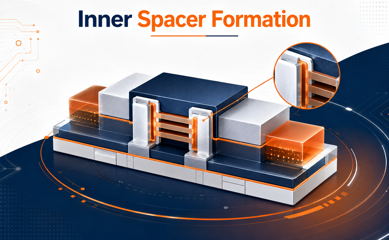
As semiconductor technology moves toward smaller process nodes, controlling the transistor structure at the nanoscale becomes increasingly important. Inner Spacer Formation is a key process step used in advanced transistor architectures such as FinFETs, Gate-All-Around (GAA) nanosheets, and nanowire transistors.
Inner spacers help control the electrical interaction between the gate and source/drain regions while maintaining precise device dimensions.
What Is Inner Spacer Formation?
An inner spacer is a dielectric layer formed between the transistor gate and the source/drain regions.
In advanced GAA structures, the inner spacer is positioned around the channel and underneath the gate-edge region. Its primary purpose is to create physical and electrical separation between the gate and source/drain extensions.
At extremely small dimensions, even a few nanometers of variation can significantly affect transistor performance, making inner spacer formation a highly controlled process.
Why Are Inner Spacers Important?
Inner spacers play several important roles in advanced transistor design:
- Reduce parasitic capacitance between gate and source/drain
- Control gate-to-source/drain overlap
- Improve electrical isolation
- Help maintain the required effective channel length
- Support better short-channel control
- Enable precise source/drain formation
As transistor dimensions shrink, controlling these effects becomes increasingly important for achieving high performance and low power consumption.
Key Process Challenges
Inner spacer formation becomes increasingly challenging as device dimensions continue to scale.
Dimensional Control
The spacer thickness must be precisely controlled. Excessive thickness can affect device dimensions, while insufficient thickness can increase unwanted electrical coupling.
Selective Etching
The process must remove the target material without damaging the channel or surrounding structures.
Uniformity
Consistent spacer dimensions across the wafer are essential for maintaining transistor-to-transistor performance.
Material Integration
The dielectric must provide the required electrical isolation while remaining compatible with subsequent fabrication processes.
Conclusion
Inner Spacer Formation is a small but highly critical process step in advanced semiconductor manufacturing.
By providing controlled isolation between the gate and source/drain regions, inner spacers help reduce parasitic effects, maintain dimensional accuracy, and support improved transistor performance.
As the industry continues to move toward GAA nanosheets, nanowires, and increasingly scaled transistor architectures, precise inner spacer formation will remain essential for achieving the required combination of performance, power efficiency, and device reliability.
Share your question in comments or talk to our mentor team for batch guidance.
Ask the Admin Team
Drop your basic question in comments: eligibility, prerequisites, tools, fee range, and placement support.
Our team reviews and responds regularly.