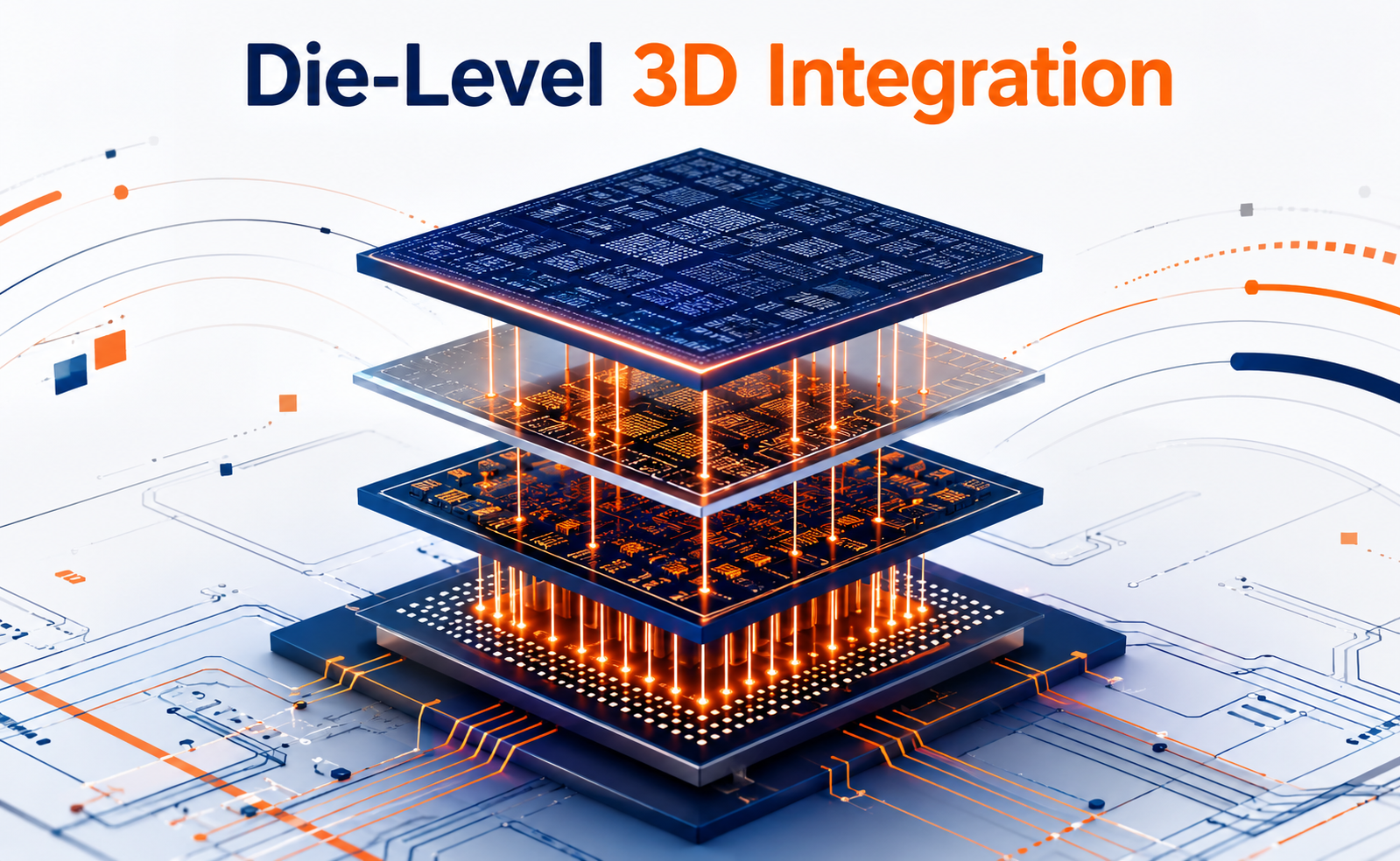
As semiconductor systems continue to demand higher performance, greater bandwidth, and improved energy efficiency, traditional 2D chip architectures are increasingly facing physical and technological limitations. Die-Level 3D Integration offers a powerful approach by vertically stacking multiple semiconductor dies and connecting them through advanced interconnect technologies.
Rather than placing all functions on a single large die, die-level 3D integration enables different dies to work together within a compact three-dimensional architecture. This approach can improve performance, reduce communication distances, and provide greater flexibility in system design.
What Is Die-Level 3D Integration?
Die-level 3D integration is an advanced packaging and integration technique in which multiple individual semiconductor dies are stacked vertically and electrically interconnected to function as a unified system.
Unlike conventional 2D integration, where components are positioned side by side on a common plane, 3D integration uses the vertical dimension to increase system density.
A typical structure may include:
Top Die → Vertical Interconnects → Bottom Die → Package/Substrate
Different dies can perform different functions, such as processing, memory, sensing, or specialized acceleration. This makes it possible to combine technologies that may not be practical to implement on a single monolithic die.
Why Is 3D Integration Important?
One of the biggest advantages of die-level 3D integration is that it addresses several challenges associated with continued semiconductor scaling.
Higher Integration Density
Stacking dies vertically allows more functionality to fit into a smaller footprint, increasing system density without requiring a proportionally larger package.
Improved Bandwidth
Shorter interconnects between dies can enable high-bandwidth communication, particularly for processor-memory architectures.
Lower Data-Movement Energy
Moving data across long distances consumes significant power. Vertical die-to-die connections can reduce interconnect lengths and therefore help improve energy efficiency.
Heterogeneous Integration
Different dies can be manufactured using different process technologies and optimized for their individual functions. These dies can then be integrated into a single 3D system.
Key Challenges in Die-Level 3D Integration
Although the technology provides significant benefits, implementing 3D integration introduces new engineering challenges.
Thermal Management:
Stacking active dies vertically can make heat removal more difficult. Effective thermal paths and advanced cooling techniques become increasingly important.
Alignment and Bonding:
As interconnect dimensions shrink, extremely precise die alignment and bonding are required to maintain reliable electrical connections.
Power Delivery:
Delivering stable power throughout a vertically stacked structure requires carefully designed power distribution networks.
Manufacturing Yield:
Multiple dies must be successfully fabricated, tested, and integrated. Defects in individual dies can affect overall system yield and cost.
Testing and Reliability:
Testing stacked structures is more complex because internal dies and interconnections may not be directly accessible after assembly.
Applications and Industry Impact
Die-level 3D integration is becoming increasingly relevant across several high-performance semiconductor applications.
AI and Machine Learning:
AI workloads require enormous amounts of data movement between compute and memory. 3D integration can help bring these functions closer together and increase bandwidth.
High-Performance Computing:
Processors and accelerators can benefit from shorter, higher-bandwidth connections between computational dies and memory.
Advanced Memory Systems:
Vertically integrated memory architectures can provide high density and bandwidth within compact packages.
Chiplet-Based Architectures:
3D integration can complement chiplet-based design by enabling multiple specialized dies to be combined within a sophisticated package.
Mobile and Edge Devices:
Higher functional density can enable powerful computing capabilities within constrained physical footprints.
The Future of Die-Level 3D Integration
Die-level 3D integration represents an important evolution in semiconductor system design. As transistor scaling becomes increasingly complex and expensive, innovation is shifting beyond the transistor itself toward advanced packaging, interconnects, and system-level integration.
Future developments are expected to focus on finer-pitch bonding, improved thermal solutions, better power delivery, advanced testing methodologies, and tighter integration between logic and memory.
Ultimately, the value of 3D integration is not simply in stacking dies—it lies in designing the entire system around vertical connectivity. By combining multiple specialized dies into a tightly integrated architecture, semiconductor engineers can create systems that deliver higher performance, greater bandwidth, improved efficiency, and increased functionality within a smaller footprint.
Conclusion
Die-Level 3D Integration is helping redefine how modern semiconductor systems are designed and packaged. By turning vertical space into an active part of chip architecture, it provides a path toward higher integration density and more efficient communication between semiconductor components.
As AI, HPC, advanced memory, and heterogeneous computing continue to grow, die-level 3D integration is positioned to play an increasingly important role in the future of semiconductor technology.
Share your question in comments or talk to our mentor team for batch guidance.
Ask the Admin Team
Drop your basic question in comments: eligibility, prerequisites, tools, fee range, and placement support.
Our team reviews and responds regularly.