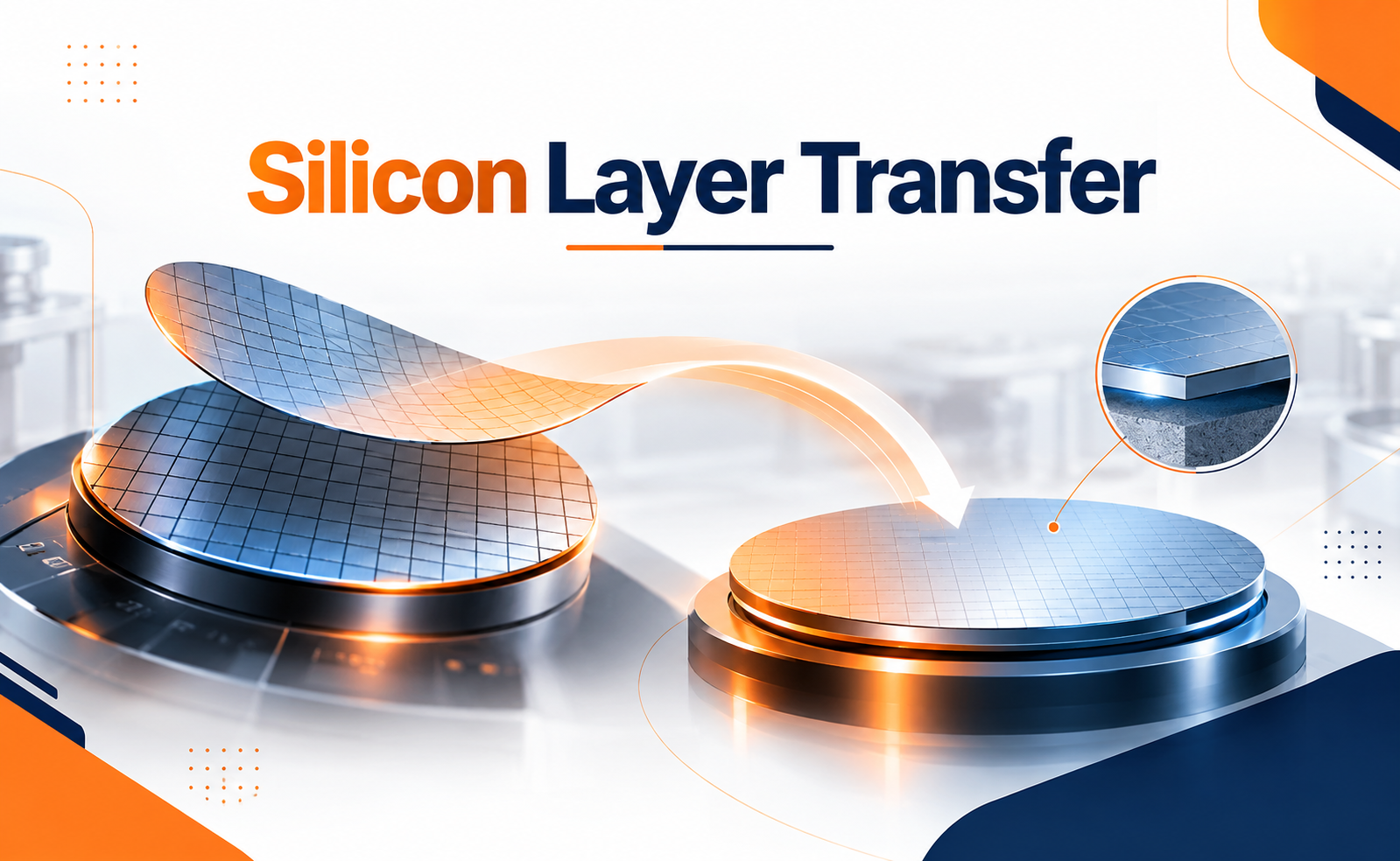
Silicon layer transfer is a critical semiconductor manufacturing technique used to move a thin, high-quality silicon layer from one substrate to another. It plays an important role in advanced device fabrication, especially where precise layer thickness, material quality, and wafer integration are essential.
What Is Silicon Layer Transfer?
Silicon layer transfer is a process in which a thin silicon layer is separated from a donor wafer and transferred onto a receiving substrate.
Instead of fabricating every device structure directly on a single bulk silicon wafer, manufacturers can create and engineer thin silicon layers independently and then integrate them with another substrate.
This approach enables better control over:
- Silicon layer thickness
- Material properties
- Electrical performance
- Device architecture
- Substrate integration
Why Is Silicon Layer Transfer Important?
Modern semiconductor devices require increasingly precise material and structural control. Silicon layer transfer provides manufacturers with a way to create specialized wafer structures that may be difficult or expensive to achieve using conventional fabrication alone.
Key advantages include:
- Thin and uniform silicon layers
- Improved device isolation
- Better control of electrical properties
- Integration with different substrate materials
- Potential reduction in material consumption
- Support for advanced device architectures
It is particularly valuable when conventional bulk-silicon processing cannot provide the required device structure.
Major Technologies Used
Several technologies can be used to achieve silicon layer transfer.
Smart Cut Technology
Smart Cut™ uses ion implantation, wafer bonding, and controlled splitting to transfer a thin silicon layer onto another substrate. It is widely associated with the production of SOI (Silicon-on-Insulator) wafers.
Wafer Bonding
Wafer bonding joins two carefully prepared surfaces. The bonding interface must have excellent cleanliness, surface flatness, and uniformity to achieve reliable integration.
Layer Splitting
Engineered regions inside the donor wafer can be separated through controlled thermal or mechanical processes, allowing the thin silicon layer to remain on the target substrate.
Epitaxial Layer Transfer
In some applications, a high-quality epitaxial silicon layer is engineered and transferred to another substrate, enabling specialized semiconductor structures.
Applications in Semiconductor Manufacturing
Silicon layer transfer supports a wide range of semiconductor technologies.
SOI Devices
Transferred silicon layers are fundamental to many SOI wafer technologies, providing electrical isolation and improved device performance.
Advanced CMOS
Thin silicon structures can support advanced transistor architectures and help improve electrostatic control.
Power Electronics
Layer-engineered silicon structures can contribute to high-voltage and power semiconductor devices.
MEMS
Silicon layer transfer can help create precisely controlled mechanical structures for sensors and microsystems.
Photonics
Transferred silicon layers are also useful for developing integrated photonic and optoelectronic platforms.
The Future of Silicon Layer Transfer
As semiconductor manufacturing moves toward smaller dimensions, 3D integration, heterogeneous integration, and advanced wafer architectures, precise layer-transfer technologies are becoming increasingly important.
Future developments will focus on:
- Higher transfer accuracy
- Lower defect densities
- Better wafer-to-wafer bonding
- Ultra-thin silicon layers
- Higher manufacturing yields
- Integration with new substrate materials
- More efficient high-volume production
Silicon layer transfer is more than simply moving silicon from one wafer to another it is an enabling technology for engineering the next generation of semiconductor devices.
Conclusion
Silicon layer transfer provides semiconductor engineers with greater flexibility in designing and manufacturing advanced wafer structures. By combining precise layer engineering, wafer bonding, controlled separation, and surface finishing, the technology enables applications ranging from SOI and CMOS to MEMS, power electronics, and silicon photonics.
Share your question in comments or talk to our mentor team for batch guidance.
Ask the Admin Team
Drop your basic question in comments: eligibility, prerequisites, tools, fee range, and placement support.
Our team reviews and responds regularly.