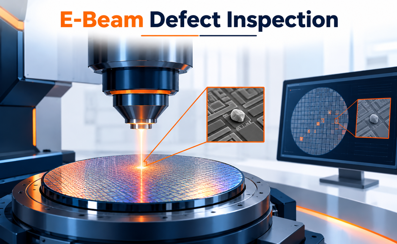
As semiconductor devices continue to shrink, identifying defects at the wafer and device level has become increasingly challenging. Conventional optical inspection methods can struggle with extremely small or low-contrast defects, creating a need for more precise inspection technologies.
E-Beam Defect Inspection, or electron-beam defect inspection, uses a focused beam of electrons to examine semiconductor surfaces and structures at very high resolution. It plays an important role in advanced process development, defect characterization, and semiconductor yield improvement.
What Is E-Beam Defect Inspection?
E-Beam Defect Inspection is a semiconductor inspection technique that uses a finely focused electron beam to scan a wafer surface and identify physical or process-related abnormalities.
Unlike optical inspection, which relies on light, e-beam inspection uses electrons to generate high-resolution images of wafer structures. This enables engineers to detect extremely small defects that may be difficult to resolve using conventional optical techniques.
Typical defects that can be investigated include:
- Pattern defects
- Particles and contamination
- Missing or extra features
- Line-edge irregularities
- Bridges and opens
- Etch-related defects
- Lithography defects
- Process-induced variations
This high-resolution capability makes e-beam inspection particularly valuable as semiconductor geometries continue to scale.
Why Is E-Beam Inspection Important?
Modern semiconductor manufacturing requires defect detection at dimensions that can approach or fall below the practical limits of traditional optical inspection.
E-beam inspection provides several important advantages:
High Resolution
The short effective wavelength associated with electron imaging enables detailed examination of very small structures.
Precise Defect Characterization
E-beam images can provide engineers with detailed information about the shape, location, and nature of a defect.
Process Development Support
During technology development, e-beam inspection can help engineers understand how fabrication processes affect device structures.
Yield Improvement
Identifying recurring defects helps manufacturers trace process problems and implement corrective actions before they significantly affect production yield.
Applications in Semiconductor Manufacturing
E-beam inspection is used across several stages of semiconductor development and manufacturing.
Lithography:
It can help identify patterning issues such as missing features, bridging, and line-edge variations.
Etch Process Monitoring:
Engineers can investigate whether etched structures have the intended dimensions and profiles.
Defect Review:
Potential defects identified by high-speed inspection systems can be examined in greater detail using e-beam techniques.
Process Development:
E-beam inspection provides detailed feedback when developing new semiconductor processes and device architectures.
Advanced Node Development:
As feature dimensions become smaller, high-resolution inspection becomes increasingly important for understanding nanoscale process variations.
The Future of E-Beam Defect Inspection
As semiconductor manufacturing moves toward increasingly advanced process nodes, defect inspection is becoming more demanding. Smaller structures require higher sensitivity, while advanced materials and complex three-dimensional architectures introduce additional inspection challenges.
Future e-beam inspection technologies are expected to focus on:
- Higher inspection throughput
- Improved defect sensitivity
- Automated defect classification
- AI-assisted image analysis
- Better handling of charging effects
- More efficient data processing
- Integration with semiconductor process-control systems
The combination of high-resolution electron imaging, automation, and intelligent data analysis can help manufacturers identify subtle process issues earlier and improve overall manufacturing control.
Conclusion
E-Beam Defect Inspection is a critical technology for high-resolution semiconductor defect detection and analysis. By using focused electron beams to examine wafer structures, it provides engineers with detailed visibility into defects and process variations that can be difficult to identify using conventional inspection techniques.
As semiconductor devices continue to become smaller and more complex, e-beam inspection will remain an important tool for defect characterization, process development, yield improvement, and advanced semiconductor manufacturing.
Share your question in comments or talk to our mentor team for batch guidance.
Ask the Admin Team
Drop your basic question in comments: eligibility, prerequisites, tools, fee range, and placement support.
Our team reviews and responds regularly.