As demand grows for faster, smaller, and more energy-efficient electronic systems, semiconductor engineers are exploring material combinations that can deliver performance beyond the limitations of conventional silicon devices. Gallium Nitride (GaN) has emerged as a key wide-bandgap semiconductor for high-frequency and high-power applications.
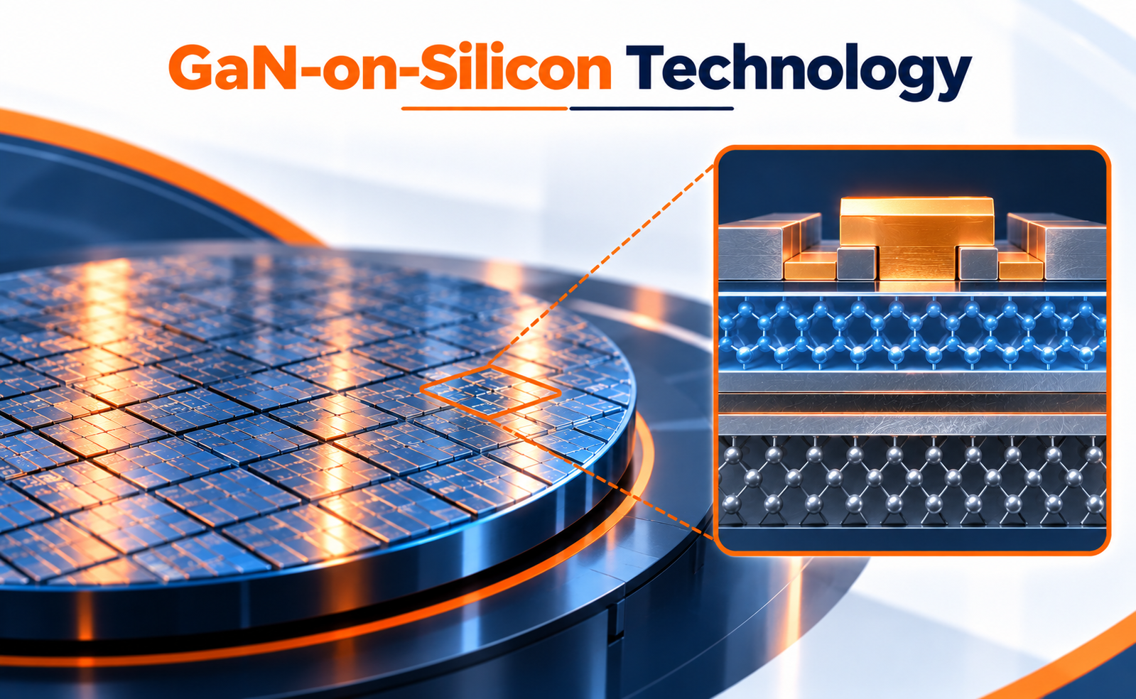
GaN-on-Silicon technology combines the electrical advantages of GaN with the scalability and manufacturing ecosystem of silicon. By growing GaN-based semiconductor layers on silicon substrates, manufacturers can develop high-performance devices while leveraging silicon-compatible wafer processing and manufacturing infrastructure.
What Is GaN-on-Silicon Technology?
GaN-on-Silicon refers to a semiconductor technology in which gallium nitride layers are epitaxially grown on a silicon substrate.
GaN offers several properties that make it attractive for power and RF electronics, including:
- Wide bandgap
- High breakdown field
- High electron mobility
- High-temperature operation capability
- High-frequency performance
- High power density
Silicon, meanwhile, provides advantages in terms of substrate availability, wafer size, cost, and established semiconductor manufacturing infrastructure.
A simplified structure can be represented as:
Silicon Substrate → Buffer Layers → GaN Layer → Active Device Structure → Metal Contacts
The combination allows GaN devices to benefit from GaN’s material properties while using silicon as the underlying platform.
Why Is GaN-on-Silicon Important?
GaN provides performance characteristics that are particularly valuable for high-power and high-frequency applications.
High Power Density
GaN devices can operate at high electric fields, allowing greater power handling within compact device footprints.
High-Frequency Operation
GaN’s electronic properties make it well suited for high-frequency switching and RF applications.
Improved Efficiency
GaN power devices can enable faster switching and lower switching losses in appropriate circuit designs, contributing to improved system efficiency.
Silicon Manufacturing Compatibility
Using silicon substrates can potentially provide access to established wafer-processing infrastructure and larger wafer formats.
Cost and Scalability Potential
GaN-on-silicon can offer a pathway toward scalable manufacturing compared with approaches that rely on more expensive or specialized substrates.
Applications of GaN-on-Silicon Technology
GaN-on-silicon is relevant to a wide range of modern electronic systems.
Power Electronics:
GaN transistors can be used in high-efficiency power converters, chargers, adapters, and power-management systems.
Data Centers:
High-efficiency GaN power devices can contribute to improved power conversion and energy management in data-center infrastructure.
RF and Wireless Communications:
GaN-based devices can support high-frequency and high-power RF applications, including wireless infrastructure and communications systems.
Automotive Electronics:
GaN technology is being explored for power conversion, onboard charging, and other high-efficiency automotive applications.
Consumer Electronics:
Compact GaN power devices enable smaller and more efficient charging solutions.
Aerospace and Defense:
The high-frequency and high-power capabilities of GaN make the material system attractive for demanding RF and electronic applications.
The Future of GaN-on-Silicon Technology
The growing demand for high-efficiency power conversion, fast charging, high-frequency communication, and electrification is creating new opportunities for GaN-based semiconductor technologies.
Future developments are expected to focus on:
- Improved GaN crystal quality
- Lower defect densities
- Better buffer-layer engineering
- Larger wafer formats
- Reduced wafer bow and stress
- Higher device breakdown performance
- Improved thermal management
- Higher manufacturing yield
- Advanced power and RF device architectures
As manufacturing processes mature, GaN-on-silicon technology has the potential to combine wide-bandgap semiconductor performance with silicon’s manufacturing scalability, making it an important platform for next-generation power and RF electronics.
Conclusion
GaN-on-Silicon Technology represents an important intersection between wide-bandgap semiconductor performance and silicon-based manufacturing. By integrating GaN with silicon substrates, engineers can develop high-performance devices capable of operating at high frequencies, high power densities, and improved efficiency.
While challenges such as lattice mismatch, thermal stress, defect control, wafer bow, and thermal management remain, continued advances in epitaxial growth and semiconductor processing are steadily improving the technology.
As industries demand more efficient power systems and increasingly capable RF electronics, GaN-on-silicon is positioned to play an important role in the future of semiconductor technology.
Share your question in comments or talk to our mentor team for batch guidance.
Ask the Admin Team
Drop your basic question in comments: eligibility, prerequisites, tools, fee range, and placement support.
Our team reviews and responds regularly.