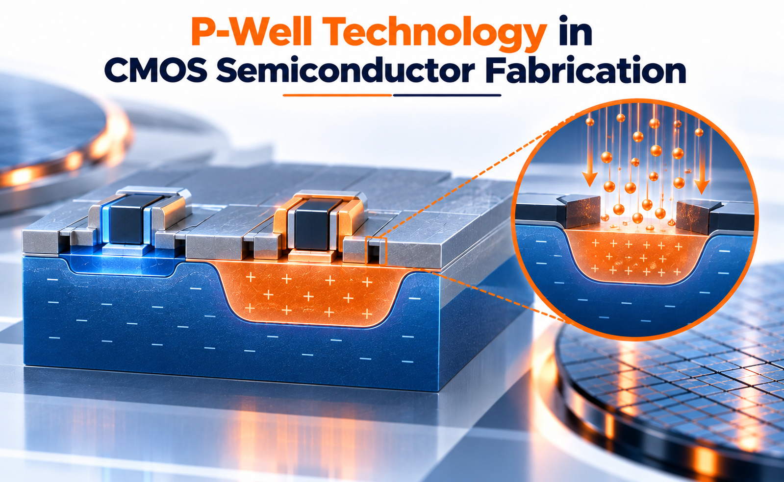
CMOS technology is one of the fundamental technologies behind modern integrated circuits, powering processors, memories, microcontrollers, sensors, and countless other electronic systems. A critical part of CMOS fabrication is the creation of well regions, which provide the appropriate semiconductor environment for forming NMOS and PMOS transistors.
P-Well Technology is an important CMOS fabrication approach in which a p-type well is formed inside an n-type semiconductor substrate. This structure provides a region where NMOS transistors can be fabricated while enabling the integration of complementary transistor types on the same chip.
What Is P-Well Technology?
P-Well Technology is a CMOS fabrication technique in which a p-type well is formed within an n-type substrate.
The p-well is created by introducing acceptor dopants into selected regions of the semiconductor. Common p-type dopants include boron and other suitable acceptor species.
A simplified structure can be represented as:
N-Type Substrate → P-Well → NMOS Formation
In a conventional p-well CMOS process, the PMOS transistor can be formed in the surrounding n-type region, while the NMOS transistor is fabricated inside the p-well.
This arrangement allows both transistor types to coexist and form the complementary logic structures that define CMOS circuits.
Role of P-Well in CMOS Devices
The p-well is more than simply a doped region—it establishes the electrical environment in which the NMOS transistor operates.
NMOS Body Formation
The p-well provides the p-type body required for an NMOS transistor.
Threshold Voltage Control
The well doping profile influences the transistor’s threshold voltage and other electrical characteristics.
Isolation
The well structure helps electrically separate device regions and contributes to controlling unwanted interactions between neighboring devices.
Latch-Up Control
Well engineering plays an important role in reducing the susceptibility of CMOS structures to parasitic effects such as latch-up.
Circuit Integration
By providing a controlled region for NMOS devices while PMOS devices are formed in the surrounding n-type region, p-well technology enables complementary CMOS circuit construction.
Advantages and Challenges of P-Well Technology
P-well technology has played an important role in the development of CMOS manufacturing and offers several benefits.
Key Advantages
Controlled NMOS Environment:
The p-well provides a carefully engineered body region for NMOS devices.
Process Flexibility:
Well doping can be adjusted to achieve desired electrical characteristics.
Improved Device Isolation:
Appropriately designed well structures can help control electrical interactions between devices.
CMOS Compatibility:
P-well technology supports the integration of NMOS and PMOS devices within a complementary circuit architecture.
Manufacturing Challenges
Dopant Profile Control:
Variations in implant dose or energy can affect well characteristics.
Junction Depth:
Precise control of well depth becomes increasingly important as device dimensions shrink.
Thermal Budget:
High-temperature processing can cause dopant diffusion and influence neighboring structures.
Latch-Up:
Poor well and substrate engineering can increase susceptibility to parasitic thyristor action.
Process Variation:
Small variations in well properties can influence transistor threshold voltage and overall circuit performance.
These challenges make ion implantation, thermal processing, metrology, and process control essential parts of p-well fabrication.
Conclusion
P-Well Technology is a fundamental concept in CMOS semiconductor fabrication. By creating a controlled p-type region within an n-type substrate, it provides the body environment required for NMOS transistor formation while supporting the complementary architecture of CMOS circuits.
From photolithography and ion implantation to dopant activation, well characterization, and device isolation, every stage requires precise process control.
As semiconductor technology advances toward increasingly sophisticated transistor structures, the principles of well engineering, doping control, junction formation, and device isolation continue to provide an important foundation for understanding modern CMOS fabrication.
Share your question in comments or talk to our mentor team for batch guidance.
Ask the Admin Team
Drop your basic question in comments: eligibility, prerequisites, tools, fee range, and placement support.
Our team reviews and responds regularly.