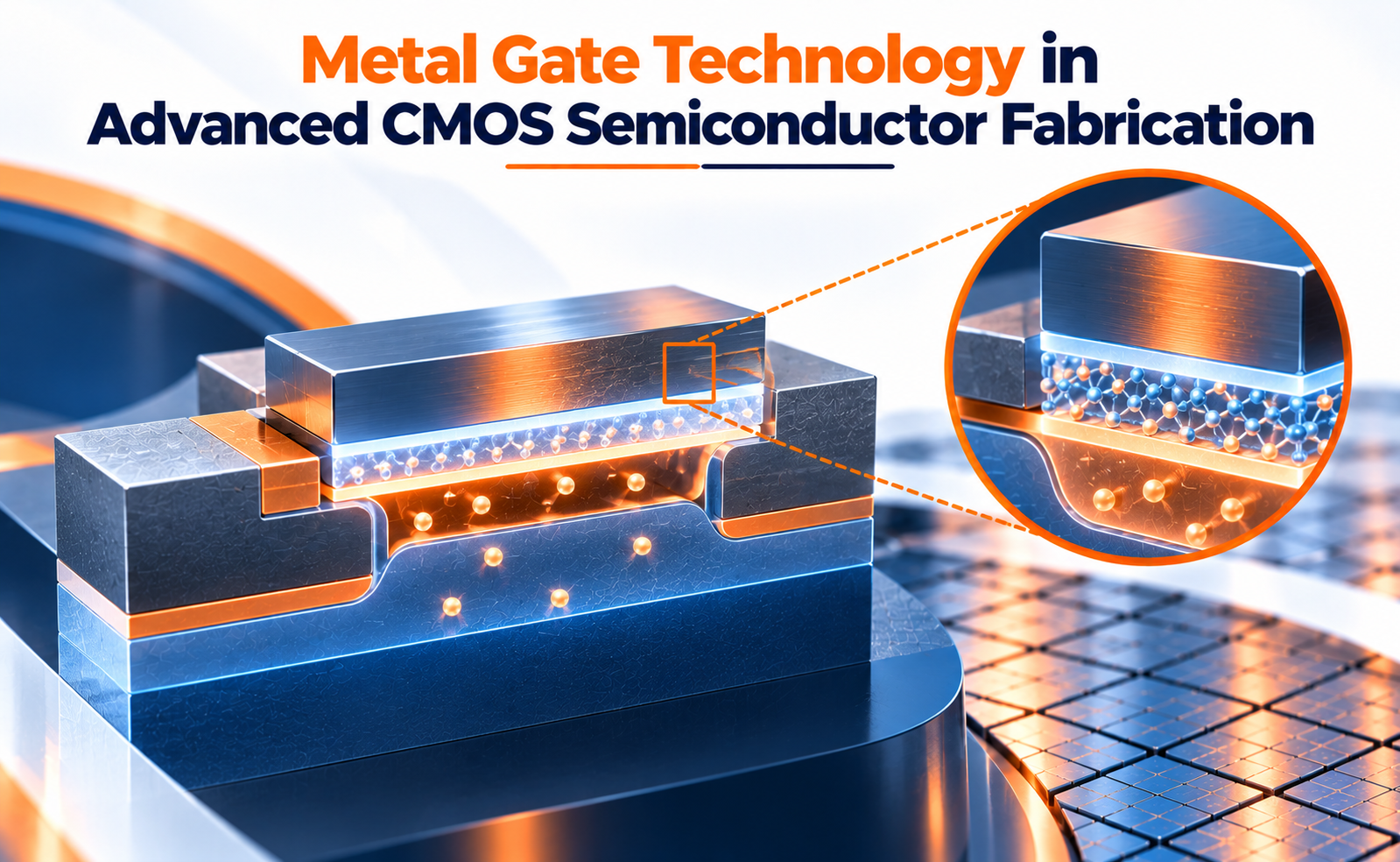
As CMOS technology continues to scale, controlling transistor performance becomes increasingly challenging. Traditional polysilicon gate structures face limitations at smaller technology nodes, particularly due to gate depletion, threshold-voltage control, and increasing gate resistance.
Metal Gate Technology has become a fundamental part of modern CMOS fabrication. By replacing polysilicon gate electrodes with metal materials, advanced transistor architectures can achieve improved electrical control and better compatibility with high-k gate dielectrics.
What Is Metal Gate Technology?
Metal Gate Technology refers to the use of a metal-based gate electrode instead of conventional polysilicon in a MOSFET.
The gate electrode works together with the gate dielectric to control the flow of carriers between the source and drain. In advanced CMOS devices, metal gates are commonly integrated with high-k dielectric materials, forming a high-k/metal-gate (HKMG) stack.
A simplified structure is:
Metal Gate → High-k Dielectric → Semiconductor Channel → Source / Drain
The metal gate material is engineered to provide an appropriate work function, which is important for controlling the transistor’s threshold voltage.
Why Did CMOS Move from Polysilicon to Metal Gates?
Earlier CMOS technologies commonly used polysilicon gates because they offered good process compatibility and allowed self-aligned source/drain formation.
However, as gate dimensions decreased and gate dielectrics became extremely thin, several limitations became more significant.
Poly Depletion
A depletion region can form in the polysilicon gate, reducing the effective gate capacitance and weakening electrostatic control.
Higher Gate Resistance
Polysilicon can have higher electrical resistance than suitable metal gate materials, which can affect switching performance.
Threshold-Voltage Challenges
Maintaining the required transistor threshold voltage becomes more difficult as dimensions shrink.
Compatibility with High-k Dielectrics
Metal gates work effectively with high-k dielectrics, enabling thicker physical dielectric layers while maintaining a high equivalent oxide capacitance.
These factors helped drive the transition toward high-k/metal-gate architectures in advanced CMOS manufacturing.
Key Advantages of Metal Gate Technology
Metal gates provide several important benefits for advanced CMOS devices.
Improved Electrostatic Control
Combined with high-k dielectrics, metal gates support strong control of the semiconductor channel while reducing gate leakage compared with very thin conventional oxide structures.
Reduced Poly Depletion
Because the gate electrode is metallic, the depletion effects associated with polysilicon gates can be avoided.
Lower Gate Resistance
Appropriately selected metal materials can provide lower resistance than polysilicon, supporting faster transistor operation.
Better Threshold-Voltage Engineering
Different metal work functions can be engineered for NMOS and PMOS devices, helping establish suitable threshold voltages.
Compatibility with Advanced Transistors
Metal-gate stacks are widely integrated with advanced transistor architectures, including FinFETs and gate-all-around (GAA) devices.
Manufacturing Challenges
Although metal gates offer significant advantages, their integration introduces complex materials and process-control requirements.
Work-Function Control:
Small variations in metal composition or interfaces can shift the transistor threshold voltage.
Interface Quality:
The interface between the high-k dielectric, metal gate, and semiconductor must be carefully controlled to minimize electrical defects.
Gate Fill:
Advanced gate structures can have narrow and complex geometries, making void-free metal filling challenging.
Thermal Stability:
The metal/high-k stack must remain stable through subsequent thermal processing.
Process Variability:
Variations in gate dimensions, dielectric thickness, metal composition, and interface properties can affect transistor performance.
Advanced thin-film deposition, etching, atomic-scale process control, metrology, and defect inspection are therefore essential for reliable metal-gate integration.
Metal Gates in the Future of CMOS
Metal gate technology continues to evolve alongside increasingly advanced transistor architectures.
Modern semiconductor development is moving toward structures such as gate-all-around nanosheet and nanowire transistors, where the gate surrounds the channel more effectively than in earlier planar architectures.
Future metal-gate development is expected to focus on:
- More precise work-function engineering
- Advanced high-k dielectric integration
- Lower gate resistance
- Improved interface quality
- Better gate-fill processes
- Reduced process variability
- Compatibility with nanosheet and nanowire devices
- Improved reliability at advanced technology nodes
The metal gate is therefore not an isolated process innovation it is a key component of the broader evolution from planar CMOS toward increasingly sophisticated three-dimensional transistor architectures.
Conclusion
Metal Gate Technology is a fundamental element of advanced CMOS semiconductor fabrication. By replacing conventional polysilicon gates with engineered metal gate stacks, semiconductor manufacturers can improve gate control, reduce poly-depletion effects, and enable effective integration with high-k dielectric materials.
From HKMG structures to FinFETs and gate-all-around transistors, metal gates continue to support the scaling of CMOS technology.
As transistor architectures become increasingly three-dimensional and feature dimensions continue to shrink, precise materials engineering, deposition, patterning, metrology, and process control will remain essential for achieving high-performance and reliable semiconductor devices.
Share your question in comments or talk to our mentor team for batch guidance.
Ask the Admin Team
Drop your basic question in comments: eligibility, prerequisites, tools, fee range, and placement support.
Our team reviews and responds regularly.