As semiconductor devices continue to shrink and become increasingly complex, manufacturing processes must provide precise control over materials at the atomic and nanometer scale. One of the most important techniques used to achieve this is Chemical Vapor Deposition (CVD).
CVD is a versatile thin-film deposition technology used to form semiconductor, dielectric, and conductive layers across a wide range of integrated-circuit manufacturing processes. Its ability to produce uniform, conformal films makes it essential for advanced CMOS, memory, power devices, and semiconductor packaging.
What Is Chemical Vapor Deposition?
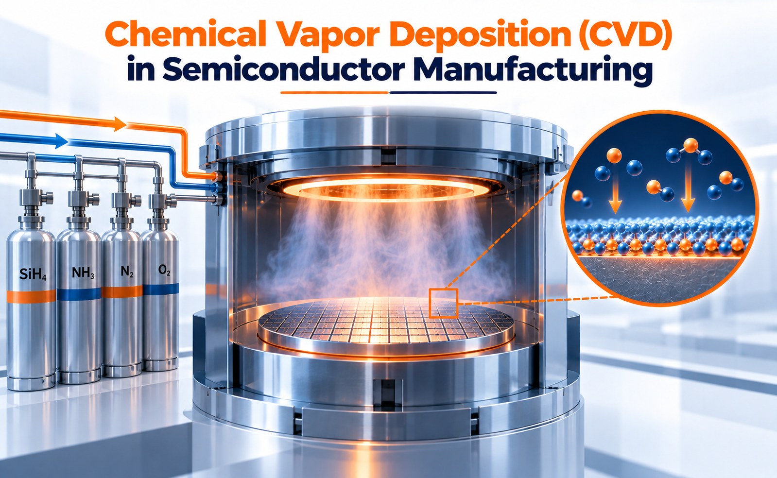
Chemical Vapor Deposition (CVD) is a thin-film deposition process in which gaseous chemical precursors are introduced into a controlled reaction chamber. These gases react or decompose at or near the surface of a heated wafer, forming a solid material on the substrate.
A simplified CVD process can be represented as:
Chemical Precursors → Reaction Chamber → Surface Reaction → Thin-Film Formation → By-Product Removal
The deposited film can consist of materials such as silicon, silicon nitride, silicon dioxide, tungsten, and other semiconductor materials.
CVD is particularly valuable because the process can deposit films over complex three-dimensional structures with good uniformity and conformality.
Types of CVD Used in Semiconductor Manufacturing
Different CVD techniques are selected according to the required film properties and process conditions.
Atmospheric Pressure CVD (APCVD)
APCVD operates close to atmospheric pressure and can provide relatively high deposition rates. It has been used for applications where high throughput is important.
Low-Pressure CVD (LPCVD)
LPCVD operates at reduced pressure and generally provides good film uniformity and conformality. It has been widely used for materials such as silicon nitride and polysilicon.
Plasma-Enhanced CVD (PECVD)
PECVD uses plasma to promote chemical reactions at relatively lower substrate temperatures. This makes it useful for depositing dielectric films where thermal budget is a concern.
Metal-Organic CVD (MOCVD)
MOCVD uses metal-organic precursors and is commonly associated with compound semiconductor manufacturing, including materials based on gallium nitride and related semiconductor systems.
The choice of CVD technique depends on factors such as film material, required thickness, deposition temperature, conformality, throughput, and device architecture.
Applications of CVD in Semiconductor Manufacturing
CVD is used throughout semiconductor fabrication to create critical material layers.
Dielectric Deposition:
CVD can deposit insulating materials such as silicon dioxide and silicon nitride for isolation, spacers, passivation, and other device structures.
Polysilicon Formation:
CVD has historically been used to deposit polysilicon for semiconductor device structures and continues to have applications in advanced fabrication.
Interconnect Processing:
Certain CVD processes are used to deposit conductive or barrier-related materials required in interconnect structures.
Spacer Formation:
Precisely controlled dielectric films can be deposited and subsequently etched to form transistor spacers.
Memory Devices:
CVD is used extensively in the fabrication of DRAM, NAND, and other memory structures where multiple thin films must be deposited with precise thickness and composition.
Compound Semiconductors:
MOCVD, a specialized form of CVD, is widely used to grow compound semiconductor layers for applications such as LEDs, RF devices, and power electronics.
The Future of CVD in Advanced Semiconductor Manufacturing
As semiconductor architectures move toward FinFETs, gate-all-around transistors, 3D memory, advanced interconnects, and heterogeneous integration, thin-film deposition requirements are becoming increasingly demanding.
Future CVD development is expected to focus on:
- Improved thickness uniformity
- Better conformal deposition in high-aspect-ratio structures
- Lower-temperature processing
- Improved precursor utilization
- Reduced particle generation
- Better control of film composition and stress
- Advanced in-situ process monitoring
- Integration with automated process-control systems
CVD is also increasingly complemented by other deposition technologies such as Atomic Layer Deposition (ALD), particularly when extremely precise and conformal films are required.
The combination of advanced deposition, metrology, and process control will be critical for maintaining manufacturing performance as semiconductor dimensions continue to shrink.
Conclusion
Chemical Vapor Deposition (CVD) is one of the foundational thin-film deposition technologies in semiconductor manufacturing. By using controlled gas-phase chemical reactions to form solid films on semiconductor wafers, CVD enables the creation of many of the critical material layers required for modern integrated circuits.
From dielectrics and polysilicon to memory structures, interconnect materials, and compound semiconductor layers, CVD supports a wide range of semiconductor manufacturing applications.
As device architectures become smaller and more three-dimensional, the ability to deposit uniform, conformal, and precisely controlled films will become increasingly important. CVD will therefore remain a key technology in the continued evolution of advanced semiconductor manufacturing.
Share your question in comments or talk to our mentor team for batch guidance.
Ask the Admin Team
Drop your basic question in comments: eligibility, prerequisites, tools, fee range, and placement support.
Our team reviews and responds regularly.