

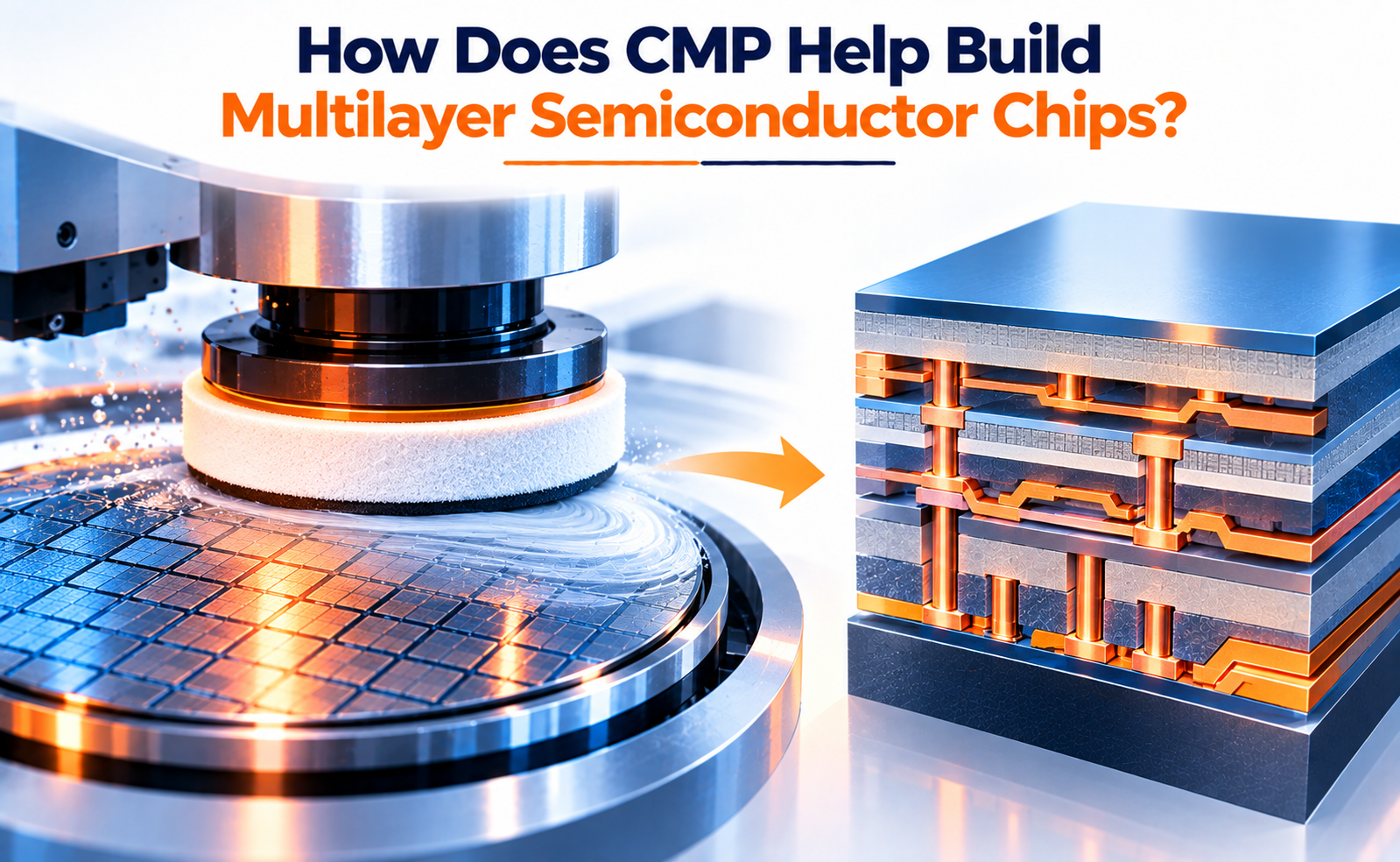
Modern semiconductor chips are no longer built as a single flat layer. Advanced integrated circuits contain multiple vertically stacked material layers, including transistors, dielectric films, contacts, vias, and metal interconnects. Building these layers reliably requires each new surface to be sufficiently flat before the next patterning and deposition steps begin.
This is where Chemical Mechanical Planarization (CMP) becomes essential.
CMP combines chemical surface modification with controlled mechanical polishing to remove material and reduce surface topography. It is widely used for both dielectric and metal layers and is a key enabling process for multilevel semiconductor manufacturing.
What Is CMP and Why Is Planarization Necessary?
Chemical Mechanical Planarization is a semiconductor manufacturing process used to make a wafer surface more uniform and planar.
During CMP, a wafer is pressed against a rotating polishing pad while a chemically active slurry is supplied to the interface. The slurry chemistry modifies the surface material, while abrasive particles and mechanical motion remove the modified material.
The need for planarization becomes more important as semiconductor chips accumulate more layers.
Without CMP, the surface would gradually develop hills, valleys, and steps created by previously patterned structures. These irregularities can create problems for subsequent:
- Lithography
- Etching
- Thin-film deposition
- Via formation
- Interconnect patterning
- Layer-to-layer alignment
A sufficiently planar surface provides a more controlled starting point for the next manufacturing stage. Research literature identifies global planarization as particularly important as feature sizes and interconnect pitches shrink.
CMP in Multilayer Interconnect Formation
One of CMP’s most important applications is the formation of the chip’s multilayer wiring system.
The interconnect structure connects individual transistors and distributes signals and power throughout the chip. Modern devices can contain multiple levels of metal interconnects separated by dielectric materials.
CMP can be applied to several materials used in these structures, including:
- Silicon dioxide and other dielectric films
- Copper
- Tungsten
- Cobalt
- Ruthenium
- Other emerging interconnect materials
CMP literature describes applications across FEOL, MOL, and BEOL processing, including shallow trench isolation, metal-gate-related processes, contacts, and multiple interconnect materials.
Why Planarity Matters for the Next Layer
The importance of CMP extends beyond simply removing excess material.
A non-planar surface can make subsequent processing increasingly difficult. Surface topography can affect photoresist coating and pattern transfer, create step-coverage problems, and complicate the formation of fine interconnect structures.
Consider a multilayer chip with several interconnect levels.
If every level leaves behind a significant amount of topography, the irregularities can accumulate as additional layers are added.
CMP essentially resets the surface profile between important process modules.
This provides several benefits:
Better Lithography
A more uniform surface helps maintain controlled photoresist thickness and improves pattern transfer conditions.
Improved Layer Integration
Planar surfaces make it easier to build subsequent dielectric, via, and metal structures.
Controlled Interconnect Geometry
CMP helps control the remaining thickness and surface profile of embedded metal features.
Higher Layer Density
By reducing accumulated topography, CMP supports the integration of multiple interconnect levels within a practical vertical structure.
Therefore, CMP is not simply a finishing operation it is an integration-enabling process that allows one layer to reliably build on another.
CMP Challenges in Advanced Multilayer Chips
As semiconductor structures become smaller and materials become more diverse, CMP itself becomes increasingly challenging.
Dishing
When polishing patterned metal structures, the center of a wide metal feature can be removed more rapidly than surrounding material, producing a recessed surface known as dishing.
Erosion
Dense patterned regions can experience greater material removal than surrounding areas, leading to local topography variations.
Scratches and Particles
Mechanical polishing and slurry particles can introduce surface defects. Post-CMP cleaning is therefore an important part of the overall process.
Selectivity
The process must remove the intended material at an appropriate rate while minimizing unnecessary removal of surrounding layers.
Low-k Dielectric Damage
Advanced interconnects increasingly use low-k dielectric materials to reduce parasitic capacitance. These materials can have different mechanical properties and may be more vulnerable to CMP-related damage.
New Interconnect Materials
As copper approaches limitations at very small dimensions, materials such as cobalt and ruthenium are being investigated and integrated into advanced interconnect schemes. Each material can require different CMP chemistry, selectivity, and process conditions.
These challenges make CMP optimization a combination of chemistry, materials science, mechanical engineering, and process control.
The Future of CMP for Advanced Semiconductor Manufacturing
As chips continue to incorporate more complex structures, CMP technology is evolving alongside them.
Future CMP development is focused on achieving extremely precise material removal while minimizing defects and protecting delicate structures.
Important development areas include:
- Advanced slurry chemistry
- Improved polishing pads
- Better endpoint detection
- Precise thickness control
- Low-defect polishing
- Advanced post-CMP cleaning
- CMP for new interconnect materials
- Improved control of wafer-level uniformity
- Modeling and simulation of material removal
- Data-driven process optimization
Recent research is also examining the dynamics of material removal and the spatial evolution of wafer topography, while new work continues to address issues such as copper corrosion during CMP.
The growing importance of CMP reflects a fundamental requirement of advanced semiconductor manufacturing: every new layer needs a well-controlled surface on which the next layer can be built.
Conclusion
CMP helps build multilayer semiconductor chips by repeatedly restoring a controlled, planar surface as different materials and interconnect layers are fabricated.
From shallow trench isolation and contacts to copper and other advanced interconnect materials, CMP supports both device integration and multilayer wiring.
Its ability to remove excess material, control surface topography, and prepare wafers for subsequent processing makes it one of the key technologies behind modern multilayer semiconductor fabrication.
As semiconductor structures continue to become smaller and more vertically integrated, the importance of CMP will extend beyond basic planarization toward precision material removal, defect control, new-material integration, and advanced process optimization.
Share your question in comments or talk to our mentor team for batch guidance.
Ask the Admin Team
Drop your basic question in comments: eligibility, prerequisites, tools, fee range, and placement support.
Our team reviews and responds regularly.