

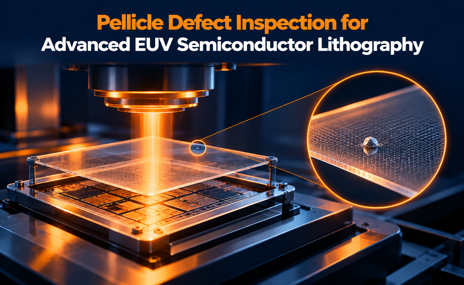
Extreme ultraviolet (EUV) lithography has become a critical patterning technology for advanced semiconductor manufacturing. As chip dimensions continue to shrink, protecting the EUV photomask from contamination becomes increasingly important.
One of the key components used for this protection is the EUV pellicle—an extremely thin membrane positioned above the photomask. Its purpose is to prevent particles from reaching the mask surface and printing unwanted defects onto the wafer.
However, the pellicle itself must also be inspected. Particles, membrane defects, holes, non-uniformities, and changes in optical properties can affect EUV transmission and ultimately influence wafer patterning. This makes pellicle defect inspection an important part of the EUV mask infrastructure and semiconductor yield-control strategy.
What Is an EUV Pellicle and Why Does It Matter?
An EUV pellicle is a very thin membrane mounted above an EUV photomask. Because the membrane is separated from the mask’s focal plane, particles landing on the pellicle can remain out of focus and are generally prevented from printing directly onto the wafer.
This protection is particularly important because an EUV mask is repeatedly used to expose many wafers. A contaminant on the mask surface can therefore become a repeating defect across multiple dies.
EUV pellicles are challenging to engineer because they must simultaneously provide:
- High EUV transmission
- Low optical impact
- Mechanical stability
- Thermal resistance
- Low contamination
- Sufficient lifetime
- Compatibility with high-vacuum EUV exposure
ASML describes EUV pellicles as extremely thin membranes that must transmit 13.5 nm EUV radiation while operating in a high-vacuum environment at elevated temperatures.
This creates an important inspection requirement: the pellicle must protect the mask without introducing significant new defects or optical variation of its own.
What Types of Defects Can Occur on an EUV Pellicle?
Pellicle inspection is not limited to finding large particles. Advanced inspection systems must identify and classify different types of physical and functional defects.
Particle Contamination
Particles can land on the front or back surface of the pellicle. Their location matters because a particle may affect the optical path differently depending on where it is positioned.
Modern inspection systems can distinguish whether detected particles are located on the front or backside of a pellicle.
Membrane Defects
The extremely thin membrane can potentially contain defects such as:
- Holes
- Tears
- Local damage
- Surface irregularities
- Thickness non-uniformity
These defects can influence the mechanical integrity or optical behavior of the pellicle.
Frame and Edge Defects
Inspection can also cover the pellicle frame and surrounding regions because contamination or damage in these areas can become a source of particles or interfere with mask handling.
Transmission and Reflectivity Non-Uniformity
Even when a pellicle appears physically intact, variations in its optical properties can matter. Specialized EUV metrology systems can map transmission and reflectivity across the pellicle.
Why Is Actinic Inspection Important for EUV Pellicles?
A major challenge in EUV inspection is distinguishing between a physical defect and a printable defect.
Not every particle or membrane imperfection necessarily produces a wafer-level failure. Its impact depends on factors such as:
- Defect size
- Defect location
- Distance from the mask
- EUV absorption
- Scattering behavior
- Local transmission
- Mask pattern geometry
- Exposure conditions
This is why inspection at the actual EUV wavelength can provide valuable information about how a defect interacts with the exposure beam.
Research at Hanyang University’s EUV Industry-University Collaboration Center has demonstrated actinic inspection approaches for EUV pellicles, including EUV ptychographic imaging and through-pellicle mask imaging to investigate defect impact.
Specialized EUV pellicle metrology can also measure spatial maps of transmission and reflection. Such measurements help determine whether the membrane has sufficiently uniform optical characteristics across its area.
The overall objective is to move from simple defect detection toward defect printability prediction.
What Are the Major Challenges in Pellicle Defect Inspection?
Inspecting an EUV pellicle is challenging because the inspection system must work with an extremely thin membrane while simultaneously maintaining high sensitivity and avoiding contamination or damage.
Extremely Thin Membranes
EUV pellicles are engineered to be exceptionally thin to maximize EUV transmission. ASML has described pellicle membranes on the order of tens of nanometers thick.
Such structures require careful handling and inspection.
Small Defect Detection
As semiconductor features become smaller, the size of defects that can affect yield also decreases. Inspection therefore needs increasingly high sensitivity.
Front-Side vs Back-Side Classification
A detected particle’s position relative to the pellicle can influence its impact. Modern systems therefore need to determine not only whether a particle exists, but also where it is located.
Optical Distortion
The pellicle itself interacts with EUV radiation. Its transmission and reflection characteristics must remain within tightly controlled limits.
CNT-based EUV pellicles, for example, have been developed with high EUV transmission and low optical influence as key objectives.
Inspection Throughput
High-volume semiconductor manufacturing requires inspection systems that combine high sensitivity with practical throughput. This becomes increasingly important as EUV lithography expands into advanced logic and future High-NA applications.
Conclusion
Pellicle defect inspection is a critical component of advanced EUV semiconductor lithography. The pellicle protects the photomask from particles, but the membrane itself must be carefully qualified to ensure that contamination, physical defects, and optical non-uniformities do not compromise wafer patterning.
Modern inspection therefore goes beyond simply looking for visible particles. It combines surface inspection, particle classification, through-pellicle inspection, EUV actinic metrology, transmission mapping, and defect printability analysis.
As EUV lithography progresses toward High-NA systems and increasingly advanced semiconductor nodes, the ability to detect smaller defects and understand their actual impact on wafer patterning will become increasingly important.
Share your question in comments or talk to our mentor team for batch guidance.
Ask the Admin Team
Drop your basic question in comments: eligibility, prerequisites, tools, fee range, and placement support.
Our team reviews and responds regularly.