

Advanced semiconductor etching processes require extremely precise control of plasma, temperature, pressure, and surface chemistry. As device dimensions shrink and plasma processes become more aggressive, controlling the wafer temperature during etching becomes increasingly important.
One of the key technologies used for this purpose is wafer backside helium cooling.
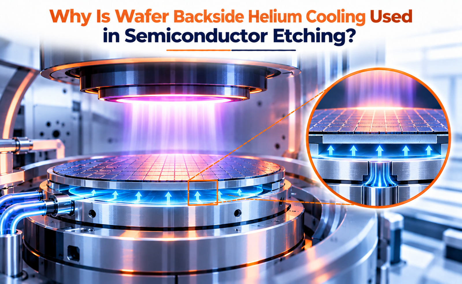
In many plasma etch systems, helium is introduced between the backside of the wafer and the electrostatic chuck (ESC). Because helium provides an effective thermal-transfer path across this very small interface, heat generated at the wafer surface can be transferred toward the cooled chuck. This helps maintain the wafer within a controlled temperature range during plasma processing.
Backside helium cooling is therefore an important part of wafer-temperature management, particularly in high-power and highly selective etching processes.
What Is Wafer Backside Helium Cooling?
During plasma etching, the front surface of a wafer is exposed to energetic ions, electrons, radicals, and other plasma species. These interactions can generate significant heat.
At the same time, the wafer is typically held on an electrostatic chuck (ESC) inside the etch chamber.
The contact between the wafer backside and the chuck is not perfectly uniform. Microscopic surface roughness and other imperfections create tiny gaps between the two surfaces. These gaps can significantly reduce direct heat transfer.
To improve thermal coupling, a controlled flow of helium is introduced into the space between the wafer and the ESC.
A simplified structure is:
Wafer → Helium backside gap → Electrostatic chuck → Cooling system
Helium is useful because it has relatively high thermal conductivity compared with many other gases and can transfer heat efficiently across the small backside gap.
The helium pressure is carefully controlled so that the wafer can remain thermally coupled to the chuck while the plasma etch process continues.
Why Is Temperature Control Important During Etching?
Wafer temperature can strongly influence plasma etching behavior.
Etching involves physical bombardment and chemical reactions at the wafer surface. These reactions can change depending on temperature, which means uncontrolled heating can alter the process outcome.
Temperature variations can affect:
- Etch rate
- Etch selectivity
- Sidewall profile
- Polymer formation
- Reaction rates
- Critical dimensions
- Surface reactions
- Etch uniformity
For example, if one region of the wafer becomes significantly hotter than another, the local etch rate may change. This can produce non-uniform feature dimensions across the wafer.
Temperature control therefore becomes especially important for advanced devices with very small features.
Backside helium cooling provides a controllable thermal path that helps remove heat generated during plasma processing and stabilizes wafer temperature.
What Are the Benefits of Helium Backside Cooling?
Backside helium cooling provides several important advantages for semiconductor etching.
Improved Temperature Uniformity
A controlled thermal interface helps maintain a more uniform wafer temperature, reducing process variation across the wafer.
Better Etch Uniformity
Because etch reactions are temperature-dependent, improved temperature control can contribute to more consistent etching across the wafer.
Stable Critical Dimensions
Temperature variations can influence feature dimensions. Thermal control therefore helps maintain more predictable critical dimensions.
Improved Process Repeatability
Maintaining consistent thermal conditions from wafer to wafer improves process repeatability.
Higher-Power Plasma Processing
As plasma etching becomes more aggressive, greater amounts of energy can be transferred to the wafer. Efficient backside cooling helps manage this additional thermal load.
Compatibility With Advanced Etching
Modern processes increasingly require tight control over profile, selectivity, and surface reactions. Stable wafer temperature supports these requirements.
For these reasons, backside helium cooling is widely associated with advanced plasma etch and deposition equipment where precise wafer thermal management is required.
The Future of Wafer Thermal Management
As semiconductor devices continue to shrink, plasma etching is becoming increasingly demanding. High-aspect-ratio structures, advanced memory architectures, gate-all-around devices, and complex 3D structures require precise control of the plasma environment and wafer surface conditions.
Future wafer thermal-management technologies are likely to focus on:
- More precise backside helium pressure control
- Improved electrostatic-chuck designs
- Better wafer-temperature monitoring
- Advanced thermal-zone control
- Improved chuck-to-wafer thermal uniformity
- Real-time process control
- AI-assisted thermal optimization
- Advanced cooling architectures for high-power plasma processes
The increasing use of sophisticated plasma processes means that temperature management will become even more closely integrated with etch-process control.
Instead of treating cooling as a separate hardware function, advanced etch systems can increasingly optimize plasma conditions, wafer temperature, chuck temperature, and backside pressure together.
Conclusion
Wafer backside helium cooling is used in semiconductor etching because precise wafer-temperature control is essential for maintaining etch performance and uniformity.
By filling the microscopic interface between the wafer and electrostatic chuck with helium, the system creates an efficient and controllable thermal-transfer path. Heat generated during plasma processing can then be transferred toward the temperature-controlled chuck.
This helps improve temperature uniformity, etch consistency, critical-dimension control, process repeatability, and thermal stability.
Share your question in comments or talk to our mentor team for batch guidance.
Ask the Admin Team
Drop your basic question in comments: eligibility, prerequisites, tools, fee range, and placement support.
Our team reviews and responds regularly.