Modern semiconductor devices are becoming increasingly complex, with billions of transistors integrated into a single chip. As the industry advances toward smaller technology nodes and three-dimensional device architectures, manufacturing processes must achieve exceptional precision and accuracy.
Advanced Etching Technologies have become one of the most critical steps in semiconductor fabrication. These technologies enable manufacturers to create ultra-fine patterns, high-aspect-ratio structures, and intricate device features required for today’s processors, memory chips, AI accelerators, and high-performance computing systems.
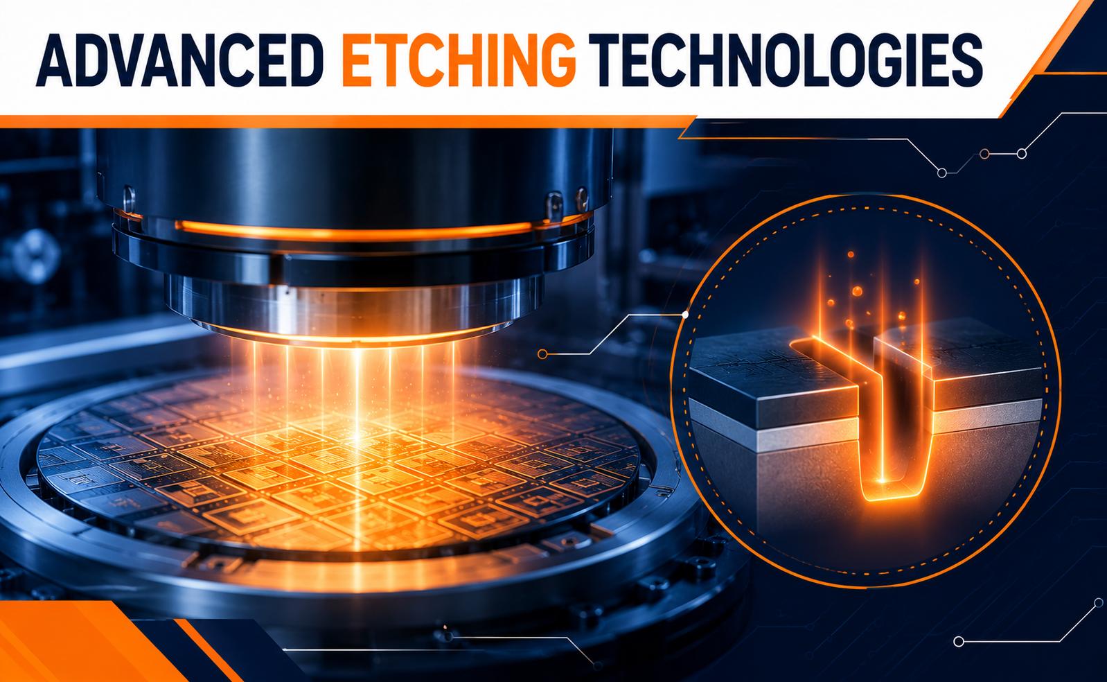
What are Advanced Etching Technologies?
Advanced Etching Technologies are semiconductor fabrication processes used to selectively remove material from a silicon wafer with extremely high precision. They transfer circuit patterns created during lithography into the underlying layers of the wafer.
Unlike conventional etching methods, advanced etching provides:
- Nanometer-scale precision
- High material selectivity
- Excellent profile control
- Minimal surface damage
- Uniform wafer processing
These capabilities are essential for manufacturing modern semiconductor devices at advanced process nodes.
Types of Advanced Etching Technologies
The semiconductor industry uses several advanced etching techniques depending on the device structure and manufacturing requirements.
Reactive Ion Etching (RIE)
Reactive Ion Etching combines plasma and chemical reactions to create highly anisotropic etching, making it suitable for fine feature patterning.
Deep Reactive Ion Etching (DRIE)
DRIE enables the creation of extremely deep and narrow structures with high aspect ratios. It is widely used in MEMS devices, advanced sensors, and Through-Silicon Via (TSV) fabrication.
Atomic Layer Etching (ALE)
ALE removes material one atomic layer at a time through cyclic processing, providing unmatched precision for advanced semiconductor nodes and Gate-All-Around (GAA) transistor manufacturing.
Plasma Etching
Plasma etching uses energized gases to selectively remove semiconductor materials while maintaining excellent process uniformity across the wafer.
Why Advanced Etching is Essential for Modern Chips
As semiconductor devices continue to shrink, etching has become increasingly challenging.
Advanced etching technologies help manufacturers achieve:
- Extremely small transistor dimensions
- High-aspect-ratio structures
- Better critical dimension (CD) control
- Improved pattern accuracy
- Reduced line-edge roughness
- Higher manufacturing yield
Without advanced etching, today’s leading-edge semiconductor technologies would not be possible.
Applications in Semiconductor Manufacturing
Advanced etching technologies are used throughout semiconductor fabrication and support a wide range of device architectures.
Major applications include:
Advanced Logic Devices
Fabrication of FinFET and Gate-All-Around (GAA) transistors for high-performance processors.
Memory Manufacturing
Production of DRAM and 3D NAND Flash memory with complex vertical structures.
Advanced Packaging
Formation of Through-Silicon Vias (TSVs), redistribution layers, and chiplet interconnections used in 2.5D and 3D packaging.
MEMS and Sensors
Manufacturing accelerometers, pressure sensors, microphones, gyroscopes, and other microelectromechanical systems requiring deep silicon etching.
The Future of Advanced Etching Technologies
As semiconductor manufacturing moves toward sub-2nm process nodes, advanced etching technologies will continue to evolve.
Future trends include:
- Greater adoption of Atomic Layer Etching (ALE)
- AI-driven process monitoring and optimization
- Advanced plasma source technologies
- Precision etching for Gate-All-Around and CFET architectures
- Enhanced support for chiplet integration and heterogeneous packaging
- Improved sustainability through reduced chemical consumption and higher process efficiency
These advancements will enable semiconductor manufacturers to produce smaller, faster, and more energy-efficient chips for future computing platforms.
Conclusion
Advanced Etching Technologies are fundamental to modern semiconductor fabrication, enabling the precise pattern transfer and material removal required for today’s most advanced chips. From logic processors and memory devices to AI accelerators and advanced packaging, these technologies make next-generation electronics possible.
As transistor architectures become more sophisticated and manufacturing scales continue to shrink, advanced etching will remain a cornerstone of semiconductor innovation, driving the performance, efficiency, and reliability of future electronic systems.
Share your question in comments or talk to our mentor team for batch guidance.
Ask the Admin Team
Drop your basic question in comments: eligibility, prerequisites, tools, fee range, and placement support.
Our team reviews and responds regularly.
