

As semiconductor technology continues to scale toward advanced process nodes, transistor performance is no longer the only factor limiting chip speed and power efficiency. The interconnect network that connects billions of transistors has become increasingly important. As metal lines become narrower and closer together, resistance and capacitance increase, resulting in higher signal delay and power consumption.
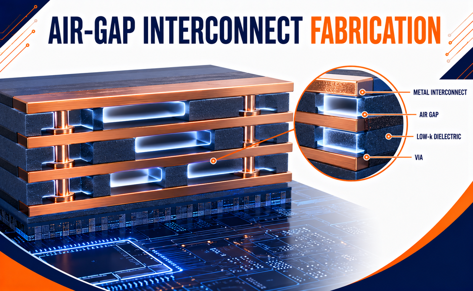
Air-Gap Interconnect Fabrication is an advanced semiconductor manufacturing technique that introduces tiny regions of air or vacuum between neighboring interconnect structures. Because air has a much lower dielectric constant than conventional insulating materials, these gaps can significantly reduce parasitic capacitance and improve signal propagation.
This technology is particularly attractive for advanced logic devices where interconnect delay and power consumption are major challenges.
What is Air-Gap Interconnect Fabrication?
Air-Gap Interconnect Fabrication is a semiconductor process technology that creates controlled empty spaces between selected metal interconnects or wiring structures.
In conventional interconnects, metal lines are surrounded by dielectric materials. These materials electrically isolate adjacent wires but also contribute to parasitic capacitance.
Air has a dielectric constant close to 1, substantially lower than most conventional interlayer dielectric materials. Replacing portions of the dielectric with air therefore reduces the electrical coupling between neighboring interconnects.
A typical air-gap interconnect structure includes:
- Metal interconnect lines
- Low-k or ultra-low-k dielectric layers
- Precisely engineered air cavities
- Etch-stop or sealing layers
- Via structures
- Barrier and liner materials
The objective is to create air gaps without compromising mechanical stability or interconnect reliability.
Why Air-Gap Technology is Important
As interconnect dimensions shrink, parasitic capacitance becomes an increasingly significant limitation.
Air-gap technology helps address this problem by reducing the dielectric material between neighboring conductors.
Key advantages include:
- Lower parasitic capacitance
- Reduced signal delay
- Lower dynamic power consumption
- Reduced electrical coupling
- Improved signal integrity
- Higher interconnect performance
- Better energy efficiency
- Support for advanced semiconductor nodes
Reducing capacitance is especially important in high-speed processors where signals must travel across increasingly dense interconnect networks.
Applications of Air-Gap Interconnects
Air-gap interconnect technology is particularly useful in advanced semiconductor systems where interconnect performance is critical.
Advanced Logic Processors
Air gaps can reduce interconnect capacitance in CPUs, GPUs, and AI accelerators, helping improve speed and energy efficiency.
High-Performance Computing
HPC processors contain extremely dense wiring networks. Lower interconnect capacitance can help reduce communication delays and power consumption.
AI Accelerators
AI workloads involve massive amounts of data movement. Improving interconnect efficiency can contribute to better overall system performance.
High-Speed Networking Chips
Switches, routers, and communication processors benefit from reduced parasitic effects in high-frequency signal paths.
Advanced Memory and 3D Integration
Air-gap concepts can also be explored in dense interconnect structures used in advanced packaging and emerging 3D semiconductor architectures.
The Future of Air-Gap Interconnect Fabrication
As semiconductor scaling continues, air-gap technology is expected to become increasingly important for managing interconnect parasitics.
Future developments may include:
- Smaller and more precisely controlled air cavities
- Integration with ultra-low-k dielectric materials
- AI-assisted process optimization
- Advanced lithography and etching techniques
- Improved mechanical reinforcement structures
- Integration with advanced 3D interconnect architectures
- Enhanced reliability monitoring and metrology
- Greater use in high-performance computing and AI hardware
Conclusion
Air-Gap Interconnect Fabrication is an important technology for addressing the growing impact of parasitic capacitance in advanced semiconductor devices. By replacing portions of conventional dielectric material with air, manufacturers can reduce capacitance, improve signal propagation, lower power consumption, and enhance overall interconnect performance.
As transistor scaling continues and chip designs become increasingly interconnected, innovations in interconnect technology will be just as important as transistor architecture. Air-gap structures therefore represent a promising approach for building faster, more energy-efficient semiconductor devices for AI, HPC, networking, and next-generation computing applications.
Share your question in comments or talk to our mentor team for batch guidance.
Ask the Admin Team
Drop your basic question in comments: eligibility, prerequisites, tools, fee range, and placement support.
Our team reviews and responds regularly.