

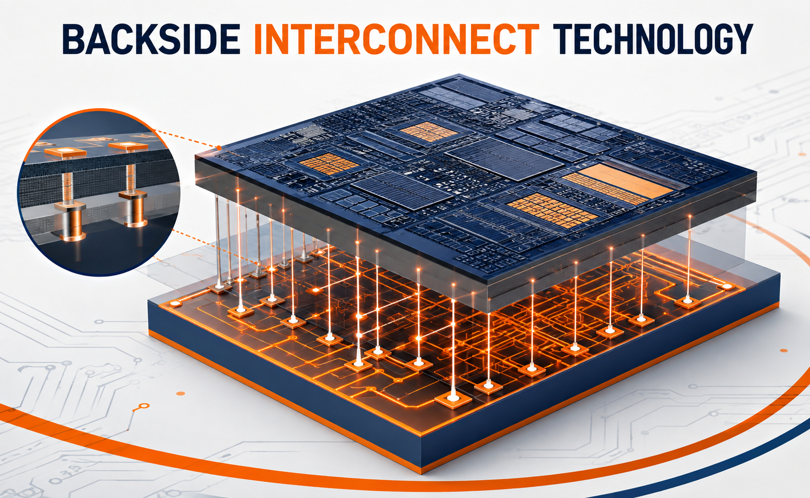
As semiconductor devices continue to scale, traditional frontside interconnects are becoming increasingly constrained by routing congestion, power delivery challenges, and signal integrity limitations. Backside Interconnect Technology is emerging as a promising approach to overcome these challenges by moving critical power and interconnect structures to the backside of the semiconductor wafer.
By separating power delivery from signal routing, backside interconnects can improve transistor utilization, reduce electrical resistance, and create new opportunities for advanced chip architectures.
What Is Backside Interconnect Technology?
Backside Interconnect Technology refers to the integration of electrical connections and power-delivery structures on the backside of a semiconductor wafer, rather than relying entirely on the conventional frontside metal stack.
In traditional chip designs, transistors and both signal and power connections are accessed from the same side. As transistor dimensions shrink, the frontside becomes increasingly crowded.
Backside interconnect technology changes this approach by creating a dedicated path for power delivery and, in some implementations, additional signal connections. This architectural separation can help semiconductor designers make more efficient use of the limited space available on advanced process nodes.
Why Backside Interconnects Are Needed
Continued scaling has created several challenges for conventional interconnect architectures:
- Increasing frontside routing congestion
- Higher resistance in power-delivery networks
- Greater voltage drop across the chip
- Increasing interconnect RC delay
- Limited space for additional routing resources
- Growing power-density requirements
- More demanding performance requirements from AI and high-performance computing
One of the major challenges is power delivery. When power must travel through increasingly complex frontside metal networks, resistance and voltage drop can negatively affect transistor performance.
Moving portions of the power-delivery network to the backside provides an additional degree of freedom in chip design and allows signal and power networks to be optimized more independently.
Key Benefits for Advanced Semiconductor Designs
Backside interconnect technology can provide several important advantages.
Improved Power Delivery
A backside power network can shorten the electrical path between the power source and transistors. This can reduce resistance and voltage drop, helping maintain more stable operating voltages.
Reduced Frontside Congestion
With power connections moved away from the frontside routing layers, more frontside resources can be dedicated to signal connections. This can simplify routing in highly dense designs.
Better Performance
Lower interconnect resistance and improved power delivery can contribute to improved electrical performance, particularly in high-performance computing architectures.
Improved Area Efficiency
Freeing frontside routing resources can provide additional flexibility for placing and connecting transistors, potentially supporting greater logic density.
Potential Power Efficiency
More efficient power distribution can reduce certain resistive losses and improve the overall power-delivery network, an important consideration for processors and AI accelerators.
The Future of Backside Interconnect Technology
Backside interconnect technology is becoming an important part of the industry’s strategy for extending semiconductor scaling beyond conventional frontside approaches.
Its importance is particularly relevant to AI accelerators, high-performance processors, data-center hardware, and other power-intensive computing systems, where performance and energy efficiency are tightly connected.
As semiconductor manufacturing progresses toward increasingly advanced process technologies, backside power delivery and interconnect architectures can provide designers with greater freedom to optimize power, signal routing, density, and performance.
Conclusion
Backside Interconnect Technology represents a fundamental shift in how advanced chips can be connected and powered. By moving critical interconnect functions to the backside of the wafer, semiconductor manufacturers can reduce frontside congestion, improve power delivery, and create additional design flexibility.
As transistor scaling continues, technologies that rethink traditional interconnect architectures will play an increasingly important role in enabling the next generation of high-performance and energy-efficient semiconductor devices.
Share your question in comments or talk to our mentor team for batch guidance.
Ask the Admin Team
Drop your basic question in comments: eligibility, prerequisites, tools, fee range, and placement support.
Our team reviews and responds regularly.