

As semiconductor technology advances toward 2nm, 1.8nm, and beyond, chip manufacturers face growing challenges in delivering power efficiently while maintaining high performance and reducing power consumption. Traditional front-side power routing consumes valuable routing space and increases electrical resistance, making it difficult to meet the demands of modern processors, AI accelerators, and high-performance computing (HPC) devices.
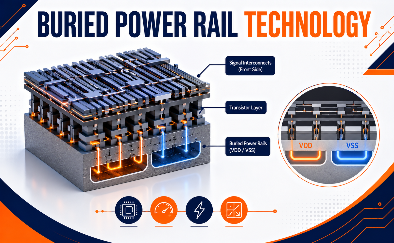
Buried Power Rail (BPR) Technology is an innovative semiconductor interconnect architecture that relocates power delivery lines beneath the transistor layer. By separating power and signal routing, BPR significantly improves routing efficiency, reduces voltage drop, enhances chip performance, and enables further transistor scaling. This technology is becoming a key enabler for future semiconductor nodes and advanced logic devices.
What is Buried Power Rail (BPR) Technology?
Buried Power Rail (BPR) is an advanced power distribution technique in which power rails (VDD and VSS) are embedded beneath the active transistor layer instead of being routed through the conventional metal interconnect layers.
Unlike traditional power delivery methods that share routing resources with signal interconnects, BPR creates a dedicated underground network for power distribution. This separation allows more routing resources for signal wiring and improves overall chip efficiency.
Why Buried Power Rail Technology is Important
As transistor dimensions continue shrinking, power delivery becomes one of the biggest challenges in semiconductor design.
Buried Power Rail Technology provides several major advantages:
- Frees routing space for signal interconnects
- Reduces IR (voltage) drop
- Lowers electrical resistance
- Improves power delivery efficiency
- Enables higher transistor density
- Enhances chip performance
- Reduces overall power consumption
- Supports advanced process nodes below 2nm
Applications of Buried Power Rail Technology
Buried Power Rail Technology is expected to play a vital role in many advanced semiconductor applications.
Artificial Intelligence (AI) Processors
Supports high-current delivery for AI accelerators while improving power efficiency.
High-Performance Computing (HPC)
Reduces power losses and enables faster processor performance in data centers and supercomputers.
Mobile Processors
Improves battery life and thermal efficiency for smartphones and tablets.
Automotive Electronics
Provides reliable power delivery for autonomous driving systems and advanced vehicle processors.
Advanced Logic Devices
Enables next-generation CPUs, GPUs, networking chips, and custom silicon manufactured using sub-2nm technologies.
The Future of Buried Power Rail Technology
Buried Power Rail is expected to become a standard feature in future semiconductor manufacturing as device scaling continues.
Emerging developments include:
- Integration with Backside Power Delivery Networks (BSPDN)
- Compatibility with RibbonFET and Gate-All-Around transistors
- AI-assisted power network optimization
- Advanced copper and ruthenium interconnect materials
- Improved thermal management techniques
- Higher-density chiplet architectures
- Enhanced power integrity for 3D integrated circuits
- Support for sub-2nm and Angstrom-era semiconductor technologies
Conclusion
Buried Power Rail (BPR) Technology represents one of the most significant advancements in semiconductor power delivery architecture. By relocating power rails beneath the transistor layer, BPR improves routing efficiency, reduces electrical losses, enhances performance, and enables continued transistor scaling for future technology nodes.
As the semiconductor industry moves toward AI computing, high-performance processors, advanced mobile devices, and heterogeneous integration, Buried Power Rail Technology will play a critical role in delivering the power efficiency and performance required for tomorrow’s integrated circuits. It is set to become a foundational innovation in the future of semiconductor manufacturing.
Share your question in comments or talk to our mentor team for batch guidance.
Ask the Admin Team
Drop your basic question in comments: eligibility, prerequisites, tools, fee range, and placement support.
Our team reviews and responds regularly.