
Why Is the Industry Looking Beyond GAA?
The semiconductor industry has continuously evolved transistor architectures to keep chips faster, smaller, and more power-efficient. After the shift from FinFETs to Gate-All-Around (GAA) transistors, engineers are already exploring the next breakthrough: Complementary Field-Effect Transistors (CFETs).
As chipmakers approach the physical limits of traditional scaling, simply shrinking transistors is no longer enough. The industry needs new architectures that can pack more transistors into the same area while maintaining performance and power efficiency.
2. What Exactly Is a CFET?
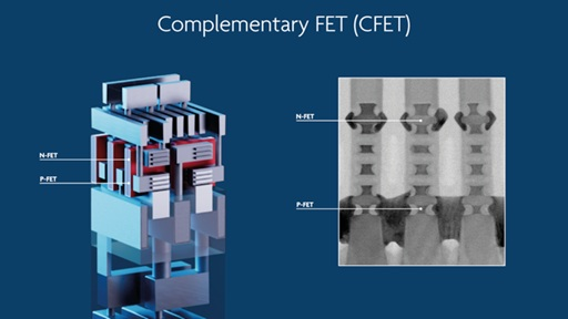
A CFET is an advanced transistor structure that vertically stacks NMOS and PMOS transistors on top of each other.
In today’s CMOS designs, NMOS and PMOS devices are placed side-by-side. CFET changes this by stacking them vertically, allowing both devices to share the same footprint.
This approach creates a true three-dimensional transistor structure, enabling significantly higher transistor density without increasing chip area.
3. Why Is CFET Important?
The biggest advantage of CFET is its ability to continue semiconductor scaling beyond the GAA era.
Key benefits include:
- Higher transistor density
- Smaller standard cell size
- Better area efficiency
- Potential power reduction
- Improved performance per square millimeter
For applications such as Artificial Intelligence (AI), High-Performance Computing (HPC), and next-generation mobile processors, these advantages could be game-changing.
4. How Does CFET Improve Chip Design?
By stacking transistors vertically, CFET reduces the amount of silicon area required for logic circuits.
This means chip designers can:
Fit more functionality into the same die size
Increase computational power
Reduce interconnect distances
Improve overall chip efficiency
In simple terms, CFET allows more computing capability without requiring larger chips.
5. What Are the Challenges?
Despite its promise, CFET is one of the most complex transistor technologies ever proposed.
Major challenges include:
- Extremely difficult manufacturing processes
- Precise alignment of stacked devices
- Heat dissipation in vertically integrated structures
- Higher fabrication costs
- Yield and reliability concerns
Before CFET becomes a mainstream technology, these manufacturing challenges must be solved at scale.
6. The Future of CFET
Many industry leaders believe CFET could become the next major transistor architecture after GAA and Forksheet devices.
Research organizations and leading semiconductor companies are actively developing CFET technology to support future process nodes beyond 2nm.
While commercial adoption may still be several years away, CFET represents one of the strongest candidates for extending Moore’s Law and enabling the next generation of AI, data-center, and high-performance computing chips.
Key Takeaway
CFET is essentially the next step after GAA transistors. By vertically stacking NMOS and PMOS devices, it enables higher transistor density, better area utilization, and continued semiconductor scaling when traditional approaches begin reaching their limits.
As the industry moves toward sub-2nm technologies, CFET is expected to play a crucial role in shaping the future of semiconductor innovation.
Share your question in comments or talk to our mentor team for batch guidance.
Ask the Admin Team
Drop your basic question in comments: eligibility, prerequisites, tools, fee range, and placement support.
Our team reviews and responds regularly.
