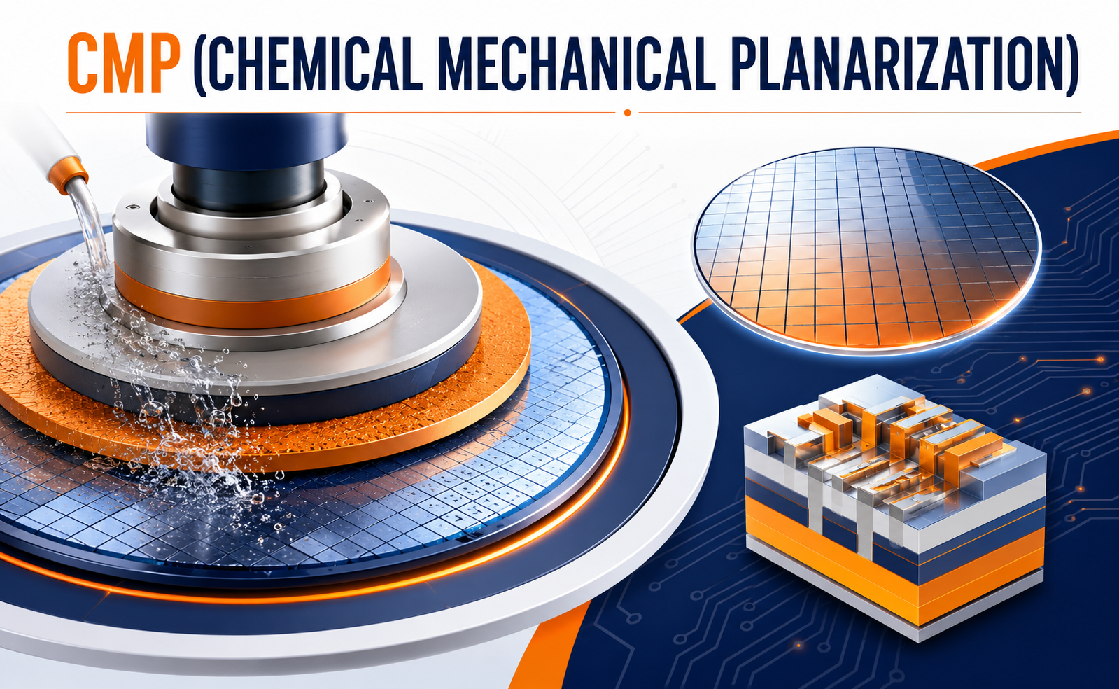
Modern semiconductor devices contain billions of transistors interconnected through multiple layers of metal and dielectric materials. As technology nodes continue to shrink below 5nm and advanced packaging becomes more complex, maintaining an extremely flat wafer surface is essential for ensuring accurate lithography, reliable interconnect formation, and high manufacturing yield.
Chemical Mechanical Planarization (CMP) is one of the most critical processes in semiconductor manufacturing. By combining controlled chemical reactions with mechanical polishing, CMP removes excess material from the wafer surface and produces exceptional planarity. This process enables the fabrication of advanced integrated circuits used in AI processors, high-performance computing, memory devices, smartphones, automotive electronics, and data center applications.
What is Chemical Mechanical Planarization (CMP)?
Chemical Mechanical Planarization (CMP), also known as Chemical Mechanical Polishing, is a wafer surface finishing process that combines chemical etching and mechanical polishing to remove excess material and create an ultra-flat surface.
During CMP, the wafer is polished using a rotating polishing pad while a specially formulated slurry containing abrasive particles and chemical reagents selectively removes material.
Why CMP is Essential in Semiconductor Manufacturing
As semiconductor fabrication involves multiple deposition and patterning steps, uneven wafer surfaces naturally develop over time.
CMP restores surface flatness, enabling accurate alignment and reliable processing throughout fabrication.
Key advantages include:
- Excellent global and local planarity
- Improved lithography focus
- Higher manufacturing yield
- Better interconnect reliability
- Uniform dielectric thickness
- Reduced defect formation
- Support for multi-layer semiconductor structures
- Compatibility with advanced technology nodes
Applications of CMP
CMP is used extensively throughout semiconductor fabrication and advanced packaging.
Shallow Trench Isolation (STI)
Creates flat isolation structures between neighboring transistors.
Interlayer Dielectric Planarization
Produces smooth dielectric surfaces before subsequent lithography and metal deposition steps.
Copper Interconnect Fabrication
Removes excess copper after electroplating in dual-damascene interconnect processes.
Through-Silicon Via (TSV) Processing
Planarizes TSV structures used in 3D integrated circuits and advanced packaging.
Advanced Packaging
Supports wafer-level packaging (WLP), fan-out packaging, chiplet integration, hybrid bonding, and 2.5D/3D semiconductor packaging technologies.
The Future of CMP Technology
As semiconductor devices become increasingly complex, CMP technology continues to evolve to meet future manufacturing demands.
Emerging innovations include:
- AI-driven CMP process optimization
- Advanced nanoparticle slurry formulations
- Improved end-point detection systems
- CMP for High-NA EUV manufacturing
- Hybrid bonding surface preparation
- Planarization of chiplet and heterogeneous integration structures
- Sustainable, low-consumption slurry technologies
- Advanced polishing solutions for sub-2nm process nodes
Conclusion
Chemical Mechanical Planarization (CMP) is a cornerstone of advanced semiconductor manufacturing, enabling the ultra-flat wafer surfaces required for precise lithography, reliable interconnect formation, and high-performance integrated circuits. By combining chemical reactions with controlled mechanical polishing, CMP ensures exceptional surface planarity throughout complex fabrication processes.
Share your question in comments or talk to our mentor team for batch guidance.
Ask the Admin Team
Drop your basic question in comments: eligibility, prerequisites, tools, fee range, and placement support.
Our team reviews and responds regularly.