

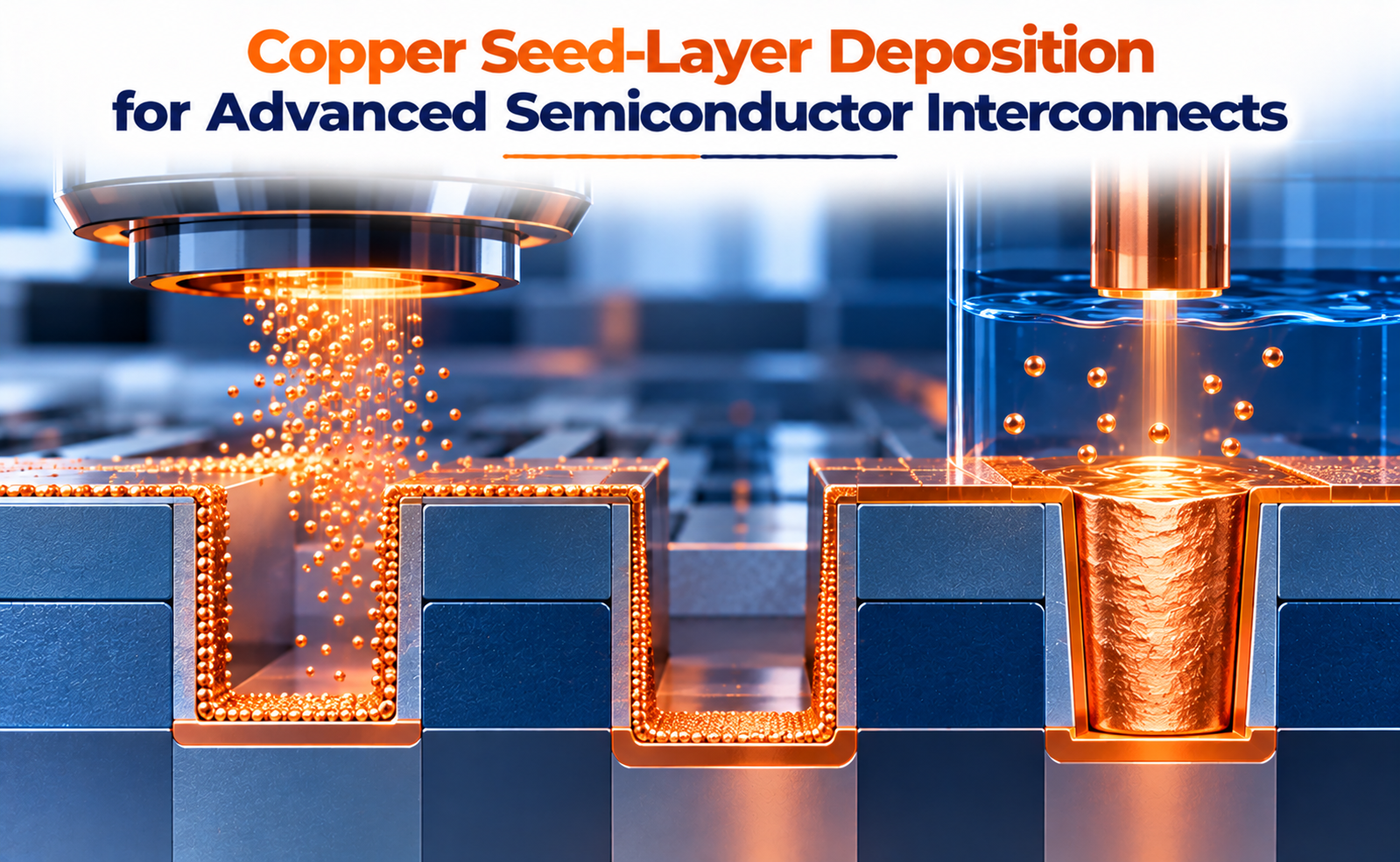
Modern semiconductor chips contain billions of transistors connected through intricate networks of microscopic metal wires. These interconnects carry electrical signals and power between different regions of the chip, making their performance essential to overall device speed and reliability.
Copper is widely used for on-chip interconnects because of its excellent electrical conductivity and suitability for damascene metallization. However, filling extremely narrow trenches and vias with copper requires a carefully engineered process. One important step is copper seed-layer deposition, which establishes a thin, conductive foundation for the subsequent electroplating process.
What Is Copper Seed-Layer Deposition?
Copper seed-layer deposition is the process of forming a thin copper film over a prepared wafer surface before bulk copper electroplating.
In a typical copper damascene process, dielectric material is patterned to create trenches and vias. A diffusion barrier or liner is then formed to prevent copper from migrating into surrounding insulating materials. Because conventional barrier materials may not provide a suitable conductive surface for direct copper electroplating, a thin copper seed layer is deposited first.
This seed layer performs several important functions:
- Provides a conductive path for electroplating current.
- Promotes copper nucleation and growth during plating.
- Supports uniform copper deposition across patterned structures.
- Helps enable complete filling of trenches and vias.
- Contributes to the electrical and structural integrity of the final interconnect.
The seed layer must be sufficiently continuous to support reliable plating, but also thin enough to preserve the available space for the final copper conductor.
How Is the Copper Seed Layer Deposited?
Several deposition technologies can be used to create copper seed layers. The most suitable method depends on feature dimensions, aspect ratio, material compatibility, and manufacturing requirements.
Physical Vapor Deposition (PVD)
PVD, particularly sputtering, is a widely used approach in which copper atoms are ejected from a target and deposited onto the wafer. It offers good process control and is compatible with established semiconductor manufacturing flows.
However, PVD is generally line-of-sight dominated. In deep, narrow trenches and vias, the upper sidewalls and feature openings may receive more material than lower regions, producing nonuniform coverage.
Chemical Vapor Deposition (CVD)
CVD forms a film through chemical reactions involving precursor gases at the wafer surface. Depending on the process chemistry, it can offer improved coverage in recessed features compared with conventional PVD.
Its challenges include precursor selection, reaction control, impurities, and integration with existing barrier and dielectric materials.
Atomic Layer Deposition (ALD)
ALD uses sequential, self-limiting surface reactions to build films in controlled increments. It can provide excellent thickness control and industry-standard lint and equivalence tools coverage in high-aspect-ratio structures.
However, copper ALD processes can face challenges involving precursor chemistry, nucleation, deposition rate, and production throughput.
Electroless Copper Deposition
Electroless deposition uses chemical reduction to deposit copper without requiring an externally applied plating current. With suitable surface preparation and activation, it can provide industry-standard lint and equivalence tools coatings on complex geometries.
Why Is Seed-Layer Uniformity Critical?
Seed-layer uniformity directly affects how copper grows during electroplating.
In an ideal process, the copper seed forms a continuous conductive film over the barrier layer, including the sidewalls and bottoms of trenches and vias. When the seed is discontinuous or excessively thin in certain regions, electrical current distribution and copper nucleation can become nonuniform.
Several defects may result:
- Voids: Empty regions remain inside the copper-filled feature.
- Seams: A narrow internal defect develops where opposing growth fronts meet.
- Pinch-off: Copper grows near the feature opening and closes it before the interior is completely filled.
- Incomplete plating: Areas with insufficient seed coverage may not receive adequate copper deposition.
- Increased resistance: Reduced copper cross-sectional area or poor connectivity can degrade electrical performance.
Seed-layer thickness must therefore be optimized carefully. An excessively thin film may be discontinuous, while an overly thick film can create overhangs near feature openings and reduce the space available for copper filling.
What Challenges Arise in Advanced Semiconductor Nodes?
As semiconductor interconnects become smaller, copper seed-layer deposition faces increasingly demanding material and process requirements.
High-aspect-ratio structures: Deep, narrow features make it difficult to achieve uniform coverage, particularly with line-of-sight deposition techniques.
Limited conductor volume: Barrier and seed layers consume part of the available feature width. As dimensions shrink, these layers can reduce the space available for the main copper conductor.
Barrier compatibility: The seed must adhere well to the underlying barrier or liner without compromising electrical performance or process stability.
Seed continuity and corrosion: Very thin copper films may be vulnerable to discontinuities or dissolution during the subsequent electroplating process, particularly in acidic plating environments.
Electrical resistance: As conductor dimensions decrease, size effects and the reduced effective copper cross-section can increase interconnect resistance.
Process integration: Deposition, plating, CMP, and thermal processing must be optimized together to achieve reliable electrical connections and high manufacturing yield.
What Is the Future of Copper Seed-Layer Technology?
Future interconnect manufacturing will require increasingly precise control over deposition at the nanoscale. Researchers and process engineers are exploring several approaches to improve copper seed-layer performance.
Advanced industry-standard lint and equivalence tools deposition: Improved CVD and ALD processes may provide more uniform coverage in narrow trenches and vias.
Alternative barrier and liner materials: Materials such as ruthenium-based systems are being investigated to reduce integration constraints and potentially simplify copper metallization.
Improved surface preparation: Better cleaning, activation, and interface engineering can support reliable nucleation, adhesion, and seed continuity.
Optimized electroplating chemistry: Improved additive systems can help achieve more uniform, void-free filling in demanding structures.
Integrated process optimization: Coordinating barrier formation, seed deposition, electroplating, and CMP can improve defect control and overall process performance.
Copper remains important in many semiconductor interconnect and advanced packaging applications. At the same time, continued scaling is encouraging research into alternative conductors and metallization schemes where conventional copper structures face increasing resistance and integration challenges.
Conclusion
Copper seed-layer deposition is a fundamental step in advanced semiconductor interconnect manufacturing. By providing a continuous conductive foundation for electroplating, the seed layer helps enable reliable copper filling of trenches and vias.
As device dimensions shrink, seed-layer continuity, thickness uniformity, barrier compatibility, and plating integration become increasingly important. Improvements in PVD, CVD, ALD, electroless deposition, and electroplating chemistry are helping address these challenges.
Ultimately, reliable seed-layer engineering supports lower defectivity, improved interconnect performance, and more manufacturable semiconductor devices.
Share your question in comments or talk to our mentor team for batch guidance.
Ask the Admin Team
Drop your basic question in comments: eligibility, prerequisites, tools, fee range, and placement support.
Our team reviews and responds regularly.