

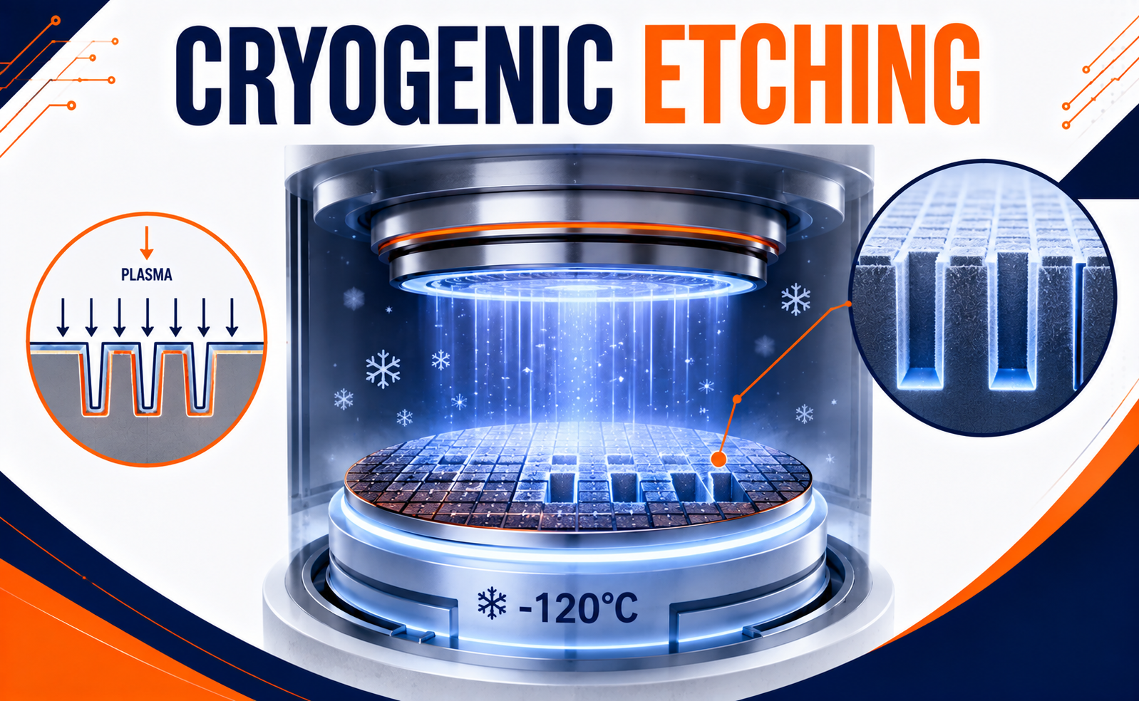
As semiconductor devices continue to shrink below the 3nm technology node, manufacturers require etching techniques capable of producing extremely fine, deep, and smooth features with exceptional precision. Conventional plasma etching methods often face challenges such as sidewall roughness, profile distortion, and reduced selectivity when fabricating nanoscale structures.
Cryogenic Etching is an advanced plasma-based semiconductor fabrication process that operates at extremely low temperatures, typically between −100°C and −150°C. By cooling the wafer during plasma etching, this technique enables highly anisotropic profiles, smoother sidewalls, and superior dimensional control. Cryogenic etching has become an important technology for manufacturing advanced logic devices, MEMS, photonic components, and next-generation transistor architectures.
What is Cryogenic Etching?
Cryogenic Etching is a dry plasma etching process in which the semiconductor wafer is cooled to cryogenic temperatures while reactive plasma removes material with exceptional precision.
Unlike conventional plasma etching, where sidewall protection is achieved using polymer deposition, cryogenic etching forms a thin passivation layer at low temperatures through controlled reactions between oxygen and silicon. This natural passivation protects the sidewalls while allowing directional material removal.
Why Cryogenic Etching is Important
Modern semiconductor devices demand deep, narrow, and highly uniform structures that are difficult to achieve using traditional etching methods.
Cryogenic Etching offers several key advantages:
- Excellent anisotropic etching
- Ultra-smooth sidewalls
- High aspect ratio capability
- Improved dimensional accuracy
- Reduced sidewall roughness (scalloping)
- Better etch selectivity
- Lower plasma-induced damage
- Higher process repeatability
Applications of Cryogenic Etching
Cryogenic Etching is widely used in advanced semiconductor and microfabrication technologies.
Gate-All-Around (GAA) Transistors
Fabricates narrow silicon nanosheets and advanced transistor structures with exceptional precision.
MEMS Devices
Creates deep trenches and microstructures used in sensors, accelerometers, gyroscopes, and pressure sensors.
Silicon Photonics
Produces precise optical waveguides and photonic devices with smooth sidewalls to minimize optical losses.
Through-Silicon Vias (TSVs)
Supports high-aspect-ratio via formation for 3D integrated circuits and advanced packaging.
Advanced Research and Nanotechnology
Used in quantum devices, nanoscale research, and next-generation semiconductor process development.
The Future of Cryogenic Etching
As semiconductor manufacturing enters the Angstrom era, cryogenic etching is expected to play an increasingly important role in advanced device fabrication.
Emerging developments include:
- AI-assisted plasma process optimization
- High-NA EUV-compatible etching techniques
- Cryogenic Atomic Layer Etching (Cryo-ALE)
- Improved temperature control systems
- Enhanced silicon photonics manufacturing
- Advanced etching for CFET and Forksheet transistor architectures
- Integration with next-generation MEMS and quantum devices
- Sustainable, energy-efficient plasma processing technologies
Conclusion
Cryogenic Etching is one of the most advanced plasma etching techniques available in semiconductor manufacturing. By combining cryogenic wafer cooling with highly controlled plasma chemistry, it delivers exceptional anisotropy, smoother sidewalls, and superior dimensional accuracy for nanoscale device fabrication.
As the industry moves toward Gate-All-Around transistors, chiplet architectures, silicon photonics, and sub-2nm process technologies, Cryogenic Etching will remain a critical enabling technology. Its ability to produce highly precise semiconductor structures with outstanding process control makes it a cornerstone of next-generation semiconductor manufacturing.
Share your question in comments or talk to our mentor team for batch guidance.
Ask the Admin Team
Drop your basic question in comments: eligibility, prerequisites, tools, fee range, and placement support.
Our team reviews and responds regularly.