

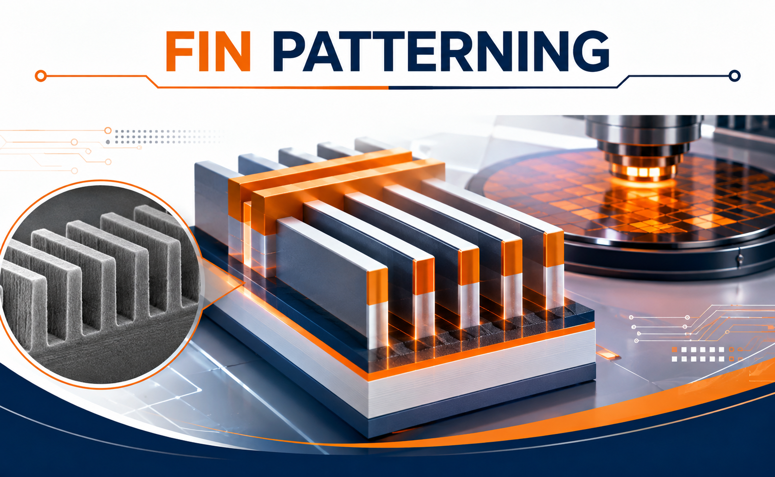
As semiconductor technology advances toward smaller process nodes, transistor architecture has evolved to improve performance, power efficiency, and device control. One of the most important developments in this evolution is the FinFET, where the transistor channel is formed as a narrow, raised silicon structure called a fin.
At the heart of this architecture is fin patterning a highly precise semiconductor manufacturing process used to define these nanoscale structures. This blog explores the fundamentals of fin patterning, its manufacturing flow, challenges, and importance in modern chip fabrication.
What Is Fin Patterning?
Fin patterning is the process of creating the narrow, raised silicon structures that form the active channels of FinFET devices.
Unlike traditional planar transistors, where the gate primarily controls the channel from above, a FinFET uses a three-dimensional fin. The gate wraps around multiple sides of this fin, providing stronger electrostatic control over the channel.
The quality of fin patterning directly influences critical device parameters such as:
- Fin width and height
- Fin spacing and pitch
- Channel dimensions
- Transistor performance
- Leakage characteristics
- Overall device variability
As dimensions shrink, maintaining precise and uniform fin structures becomes increasingly challenging.
Why Fin Patterning Matters
Modern semiconductor devices require extremely accurate feature definition. Even small variations in fin dimensions can affect transistor behavior across an entire wafer.
Effective fin patterning helps manufacturers achieve:
Better electrostatic control
The three-dimensional fin allows the gate to control the channel more effectively.
Improved power efficiency
Better channel control can help reduce unwanted leakage currents.
Higher transistor density
Precisely defined fins allow more devices to be integrated into a limited area.
Consistent device performance
Uniform fin dimensions are essential for reducing variation between transistors.
This makes fin patterning a critical step in advanced logic semiconductor manufacturing.
The Role of Advanced Lithography
As fin pitch and critical dimensions become smaller, conventional lithography techniques face increasing limitations.
Advanced patterning approaches may involve techniques such as:
- Optical lithography with multiple patterning
- Self-aligned patterning
- Spacer-based patterning
- EUV lithography in applicable process flows
The objective is not simply to print smaller features, but to achieve accurate, repeatable, and uniform structures across the wafer.
Critical dimensions such as fin width, pitch, line-edge roughness, and pattern placement must be carefully controlled because variations can translate directly into electrical differences between transistors.
Conclusion
Fin patterning enables the precise formation of the nanoscale structures that make FinFET technology possible. From lithography and pattern transfer to silicon etching and metrology, every stage must be carefully controlled to achieve consistent device performance.
As semiconductor manufacturing moves toward increasingly complex architectures, the principles developed through FinFET fin patterning will continue to influence the next generation of transistor technologies.
Share your question in comments or talk to our mentor team for batch guidance.
Ask the Admin Team
Drop your basic question in comments: eligibility, prerequisites, tools, fee range, and placement support.
Our team reviews and responds regularly.