

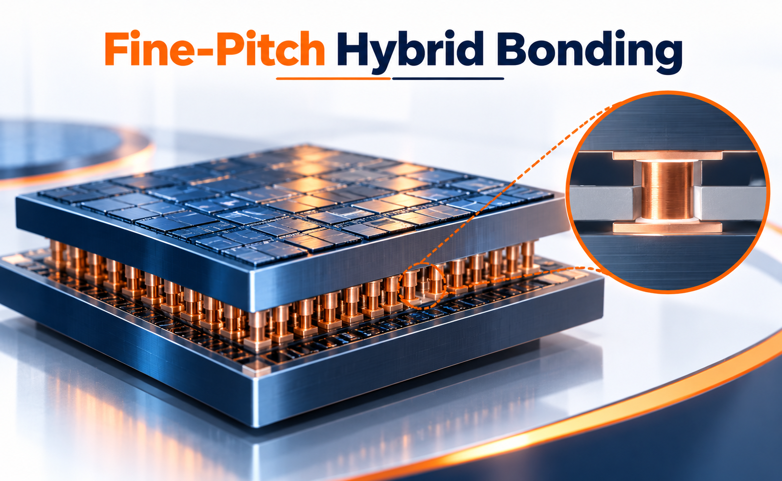
As semiconductor architectures continue to evolve, traditional interconnect technologies are increasingly challenged by the demand for higher bandwidth, greater I/O density, lower power consumption, and smaller package dimensions. Fine-Pitch Hybrid Bonding (FPHB) is emerging as a critical technology for addressing these requirements.
By combining metal-to-metal electrical connections with dielectric-to-dielectric bonding, hybrid bonding enables extremely fine interconnect pitches without relying on conventional solder-based connections. This makes it particularly valuable for advanced 3D integration, chiplet architectures, image sensors, memory, and high-performance computing.
What Is Fine-Pitch Hybrid Bonding?
Fine-Pitch Hybrid Bonding is an advanced wafer-to-wafer or die-to-wafer bonding technique that creates electrical and mechanical connections between two semiconductor surfaces without requiring conventional solder bumps.
The technology typically consists of two bonding interfaces:
- Copper-to-copper bonding for electrical interconnection
- Dielectric-to-dielectric bonding for mechanical attachment and structural support
Unlike traditional flip-chip technologies, hybrid bonding can achieve much smaller interconnect pitches, allowing a significantly greater number of connections within the same area.
A simplified structure can be represented as:
Die / Wafer → Dielectric Interface + Copper Pad → Copper Pad + Dielectric Interface → Die / Wafer
The result is a highly dense, short interconnect between semiconductor devices.
Why Is Fine-Pitch Hybrid Bonding Important?
The primary advantage of hybrid bonding is its ability to dramatically increase interconnect density while reducing the electrical distance between connected devices.
Ultra-Fine Interconnect Pitch
Hybrid bonding can support pitches significantly smaller than conventional solder-based interconnect technologies, making it suitable for highly integrated semiconductor architectures.
Higher Bandwidth
Shorter and denser connections can enable high-bandwidth communication between stacked dies or chiplets.
Lower Interconnect Power
Short electrical paths can reduce parasitic capacitance and help lower the energy required to move data between interconnected devices.
Improved Form Factor
Removing large solder bumps allows semiconductor dies to be placed closer together, supporting thinner and more compact packages.
Better 3D Integration
Hybrid bonding provides an effective foundation for vertically stacking semiconductor dies with extremely dense connections.
Applications of Fine-Pitch Hybrid Bonding
Fine-pitch hybrid bonding is particularly relevant to semiconductor applications where interconnect density and bandwidth are critical.
3D Semiconductor Integration:
Multiple semiconductor dies can be vertically stacked to create highly integrated systems with dense die-to-die connections.
Advanced Memory:
Hybrid bonding can enable high-density connections between memory structures and logic dies, supporting increased bandwidth and improved system efficiency.
Image Sensors:
Hybrid bonding is used in advanced image sensor architectures to connect sensor and logic wafers with high-density interconnects.
Chiplet-Based Architectures:
As systems increasingly use multiple specialized chiplets, fine-pitch bonding can provide efficient die-to-die communication.
High-Performance Computing and AI:
AI accelerators and HPC processors require massive data movement between compute and memory components, making high-density interconnect technologies increasingly important.
The Future of Fine-Pitch Hybrid Bonding
The semiconductor industry is moving toward increasingly heterogeneous and three-dimensional architectures. As transistor scaling becomes more difficult and expensive, advanced packaging technologies are becoming an increasingly important part of overall system scaling.
Fine-pitch hybrid bonding is positioned to support this transition through:
- Smaller interconnect pitches
- Higher die-to-die bandwidth
- Greater I/O density
- Lower interconnect power
- Advanced 3D stacking
- Chiplet integration
- Improved memory-to-logic connectivity
- More compact semiconductor packages
Future development will focus on improving bonding yield, alignment accuracy, surface preparation, defect inspection, throughput, and process control while pushing interconnect dimensions toward even finer pitches.
Conclusion
Fine-Pitch Hybrid Bonding represents a major advancement in semiconductor interconnect technology. By combining copper-to-copper electrical bonding with dielectric-to-dielectric bonding, it enables extremely dense connections between semiconductor dies and wafers.
As the industry moves toward 3D integration, chiplets, advanced memory, AI accelerators, and heterogeneous packaging, the ability to create reliable, ultra-fine-pitch interconnects will become increasingly important.
Ultimately, fine-pitch hybrid bonding is helping shift semiconductor scaling beyond the transistor itself—bringing more bandwidth, higher integration, and greater system performance into increasingly compact packages.
Share your question in comments or talk to our mentor team for batch guidance.
Ask the Admin Team
Drop your basic question in comments: eligibility, prerequisites, tools, fee range, and placement support.
Our team reviews and responds regularly.