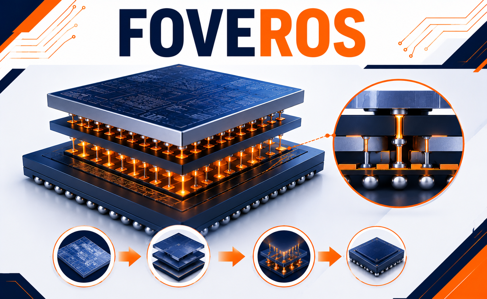
As the semiconductor industry moves beyond traditional transistor scaling, advanced packaging technologies have become essential for delivering higher performance, improved power efficiency, and greater functionality. One of the most significant innovations in this space is Foveros, Intel’s groundbreaking 3D chip stacking technology.
Foveros enables multiple semiconductor dies to be vertically stacked and interconnected using high-density interconnects, allowing logic, memory, and specialized processing units to function as a single integrated system. By leveraging true three-dimensional integration, Foveros significantly improves performance-per-watt, reduces package size, and supports heterogeneous integration, making it a key technology for AI, high-performance computing, edge computing, and next-generation consumer devices.
What is Foveros Technology?
Foveros is an advanced 3D die-stacking packaging technology that vertically integrates multiple active semiconductor dies using Through-Silicon Vias (TSVs) and fine-pitch interconnects. Unlike traditional 2D packaging, where chips are placed side by side, Foveros stacks active dies directly on top of one another, enabling shorter communication paths and higher integration density.
Why Foveros is Transforming Semiconductor Packaging
Modern processors require increasing numbers of CPU cores, AI engines, graphics units, and memory resources. Traditional packaging approaches often struggle with signal latency, power consumption, and physical size constraints.
Foveros addresses these challenges by providing:
- True 3D chip stacking
- Higher transistor density
- Reduced signal path length
- Lower communication latency
- Improved bandwidth
- Better power efficiency
- Smaller package footprint
- Support for heterogeneous integration
Applications of Foveros Technology
Foveros is designed for advanced semiconductor applications that demand exceptional performance, efficiency, and integration.
Artificial Intelligence (AI)
Supports AI processors with tightly integrated compute engines and high-bandwidth memory.
High-Performance Computing (HPC)
Improves processor scalability and communication efficiency in data centers and supercomputers.
Client and Mobile Processors
Enables compact, power-efficient processors for laptops, tablets, and ultra-portable devices.
Data Center Infrastructure
Supports advanced server processors with heterogeneous computing architectures for cloud workloads.
Edge Computing and IoT
Provides compact, energy-efficient semiconductor solutions for intelligent edge devices and industrial applications.
The Future of Foveros Technology
As semiconductor innovation increasingly focuses on advanced packaging and chiplet architectures, Foveros is expected to play an even greater role in future computing platforms.
Emerging developments include:
- Hybrid bonding integration
- Chiplet-based heterogeneous computing
- AI accelerator packaging
- Integration with High-Bandwidth Memory (HBM)
- Advanced power delivery architectures
- Next-generation 3D stacking techniques
- Co-packaged optical interconnects
- Sustainable, high-density semiconductor packaging
Conclusion
Foveros represents a major advancement in semiconductor packaging by enabling true three-dimensional integration of active semiconductor dies. Through advanced stacking techniques, high-density interconnects, and heterogeneous integration, Foveros delivers substantial improvements in performance, power efficiency, and package density.
As artificial intelligence, high-performance computing, cloud infrastructure, and edge computing continue to evolve, Foveros will remain a cornerstone technology for next-generation semiconductor design. By redefining how chips are integrated within a package, it is helping shape the future of high-performance and energy-efficient computing.
Share your question in comments or talk to our mentor team for batch guidance.
Ask the Admin Team
Drop your basic question in comments: eligibility, prerequisites, tools, fee range, and placement support.
Our team reviews and responds regularly.